Adiabatic Mode-Profile Conversion by Selective Oxidation for Photonic Integrated Circuit

Active Publication Date: 2013-01-17
INNOLUME
View PDF5 Cites 20 Cited by
  • Summary
  • Abstract
  • Description
  • Claims
  • Application Information

AI Technical Summary

Benefits of technology

[0019]The method also includes the step of selectively oxidating the mode control region, where an oxidation time and an oxidation temperature are selected such that an oxidation depth is large enough to sufficiently change an effective refractive index of the mode control region in the narrow section in order to provide mode localization in the passive region inside the narrow section. The thickness of the wide section is sufficiently high so that oxidation o

Problems solved by technology

However, the cost of the components is high mainly because of the package itself, where coupling optics, temperature stabilization, and precise adjustment are all required.
Moreover, systems based on the discrete components are power consumable and it is difficult to make them compact in size.
However, there are also disadvantages including, but not limited to, an inefficient light coupling between the components, different lattice and thermal expansion constants, and diffusion of impurities between the components.
However, the epitaxial crystal growth at the abutting locations creates the problem of layer misalignment and imperfect interfaces (quality and shape) between the active and passive components, which results in scattering loss, parasitic optical feedback, and low coupling efficiency.
However, the waveguide properties cannot be strongly changed on a short distance resulting in additional absorption losses and chirp in the region of the band edge transition.
Different modifications of the QWI technique, such as impurity free vacancy disordering (IFVD), impurity induced disordering (IID) and laser-induced disordering (LID), suffer from their specific drawbacks, including free-carrier absorption, parasitic conductivity, residual damage from implantation, inferior qu

Method used


Image

  • Adiabatic Mode-Profile Conversion by Selective Oxidation for Photonic Integrated Circuit
  • Adiabatic Mode-Profile Conversion by Selective Oxidation for Photonic Integrated Circuit
  • Adiabatic Mode-Profile Conversion by Selective Oxidation for Photonic Integrated Circuit

Examples


Example

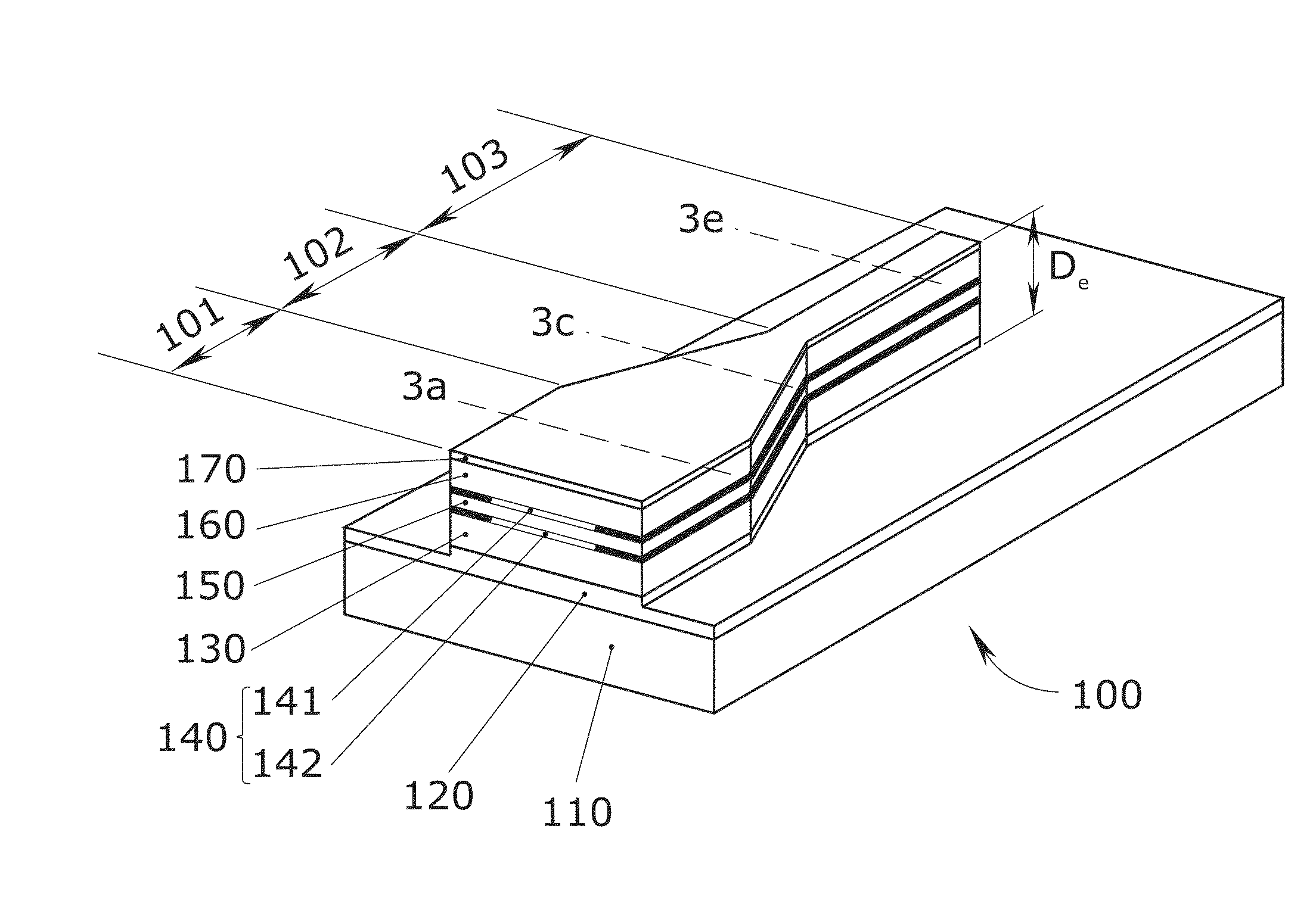
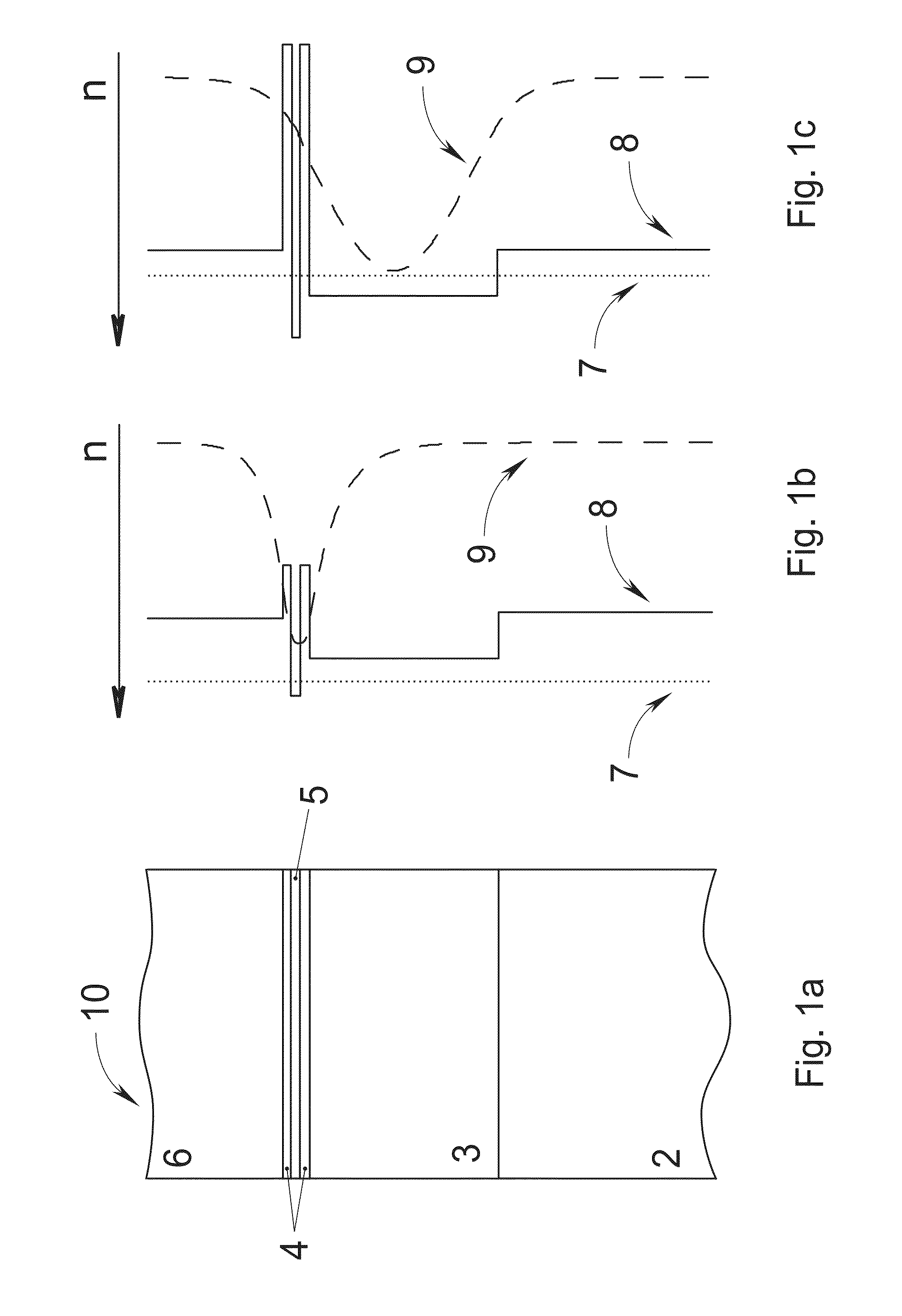
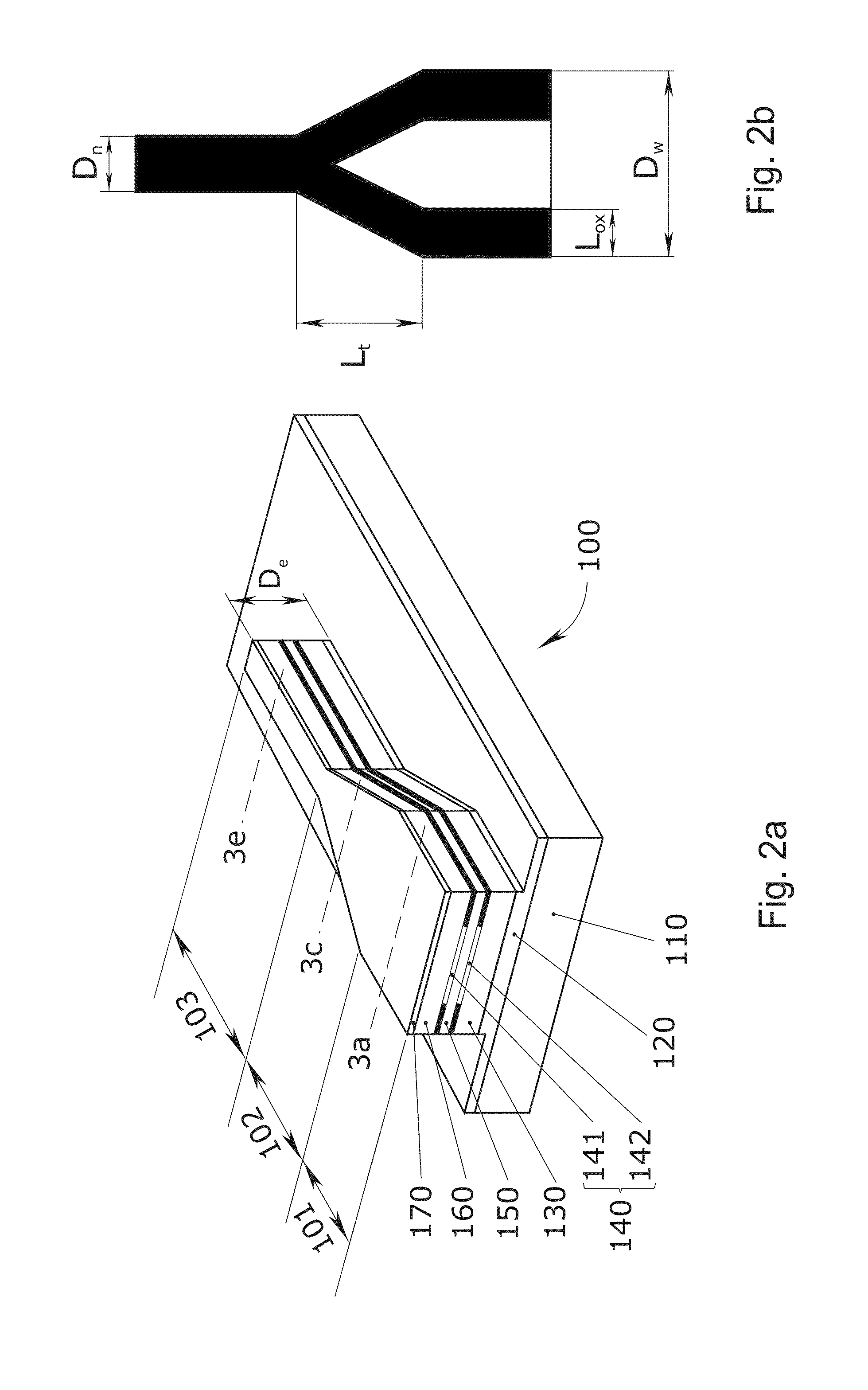
[0038]In order to overcome the drawbacks of the prior art, the waveguide design and fabrication method are based on the selective oxidation technology for adiabatic mode-profile conversion in the vertical monolithic integration of active devices with passive elements into a single photonic integrated circuit with improved manufacturability and reliability. Some optical devices for which the methods and devices of the present invention could be used include, but are not limited to, lasers, photodetectors, modulators, light emitting diodes, amplifiers, detectors, power splitters, switchers, filters, multiplexers, array waveguide gratings, and passive waveguides.

[0039]“Adiabatic”, as defined herein, means gradually or smoothly, and with negligible power losses / scattering / interference. “Adiabatic mode transformation”, as defined herein, means gradual mode transformation with negligible power losses. A “single-step ridge” and “single-step ridge waveguide”, as defined herein, are ridge st...


PUM


Abstract

Waveguide designs and fabrication methods provide adiabatic waveguide eigen mode conversion and can be applied to monolithic vertical integration of active and passive elements in PICs. An advantage of the designs and methods is a simple fabrication procedure with only a single etching step in combination with subsequent well-controllable selective oxidation. As a result, improved manufacturability and reliability can be achieved.

Description

REFERENCE TO RELATED APPLICATIONS[0001]This application claims one or more inventions which were disclosed in Provisional Application No. 61 / 507,233, filed Jul. 13, 2011, entitled “Adiabatic Mode-Profile Conversion by Selective Oxidation For Photonic Integrated Circuit”. The benefit under 35 USC §119(e) of the United States provisional application is hereby claimed, and the aforementioned application is hereby incorporated herein by reference.BACKGROUND OF THE INVENTION[0002]1. Field of the Invention[0003]This invention relates to the field of integrated optics, and more particularly to methods of monolithic integration of active devices with passive components.[0004]2. Description of Related Art[0005]Presently many optoelectronic systems are assembled from separate components that are individually packaged into fiber modules. These components include, but are not limited to, LEDs, lasers, amplifiers, modulators, detectors, power splitters, switchers, filters, and multiplexers. Howe...

Claims


Application Information

Patent Timeline
IPC IPC(8): G02B6/12H01L21/20B82Y20/00
CPCG02B6/1228G02B6/136H01S5/2215G02B2006/12097H01S5/1064G02B2006/12078
Inventor GUBENKO, ALEXEYKRESTNIKOV, IGORMIKHRIN, SERGEYLIVSHITS, DANIILWOJCIK, GREGKOVSH, ALEXEY
Owner INNOLUME
Why Eureka
Try Eureka