Gas sensor with radiation guide

a radiation guide and gas sensor technology, applied in the field of optical absorption gas sensors, can solve the problems of low cost sensor, high cost, and short path length, and achieve the effects of less technical difficulty, lower cost, and higher quality

Inactive Publication Date: 2013-01-31
GAS SENSING SOLUTIONS
View PDF2 Cites 10 Cited by
  • Summary
  • Abstract
  • Description
  • Claims
  • Application Information

AI Technical Summary

Benefits of technology

[0080]Producing a uniform film on the inner surface of an L-shaped surface is much less technically challenging than for a member comprising...

Problems solved by technology

However, the reflecting surface will introduce optical loss from absorption and/or scatter and this optical loss will typically be significant in a low cost sensor.
However, for many practical applications, it is desirable for gas sensors to be small, or to comply with standardised dimensions, resulting in generally short path lengths and corresponding low sensitivity.
It is known that for linear radiation guides increasing the size of the cross section decreases the number of reflections and therefore the absorption loss but results in poor collection efficiency.
However, where a radiation guide curves, radiation falling on the curved walls of the guide results in greater angular spread without a reduction in spatial spread and consequently an increase in loss due to absorption in the multiple reflections...

Method used


Image

  • Gas sensor with radiation guide
  • Gas sensor with radiation guide
  • Gas sensor with radiation guide

Examples


example 1

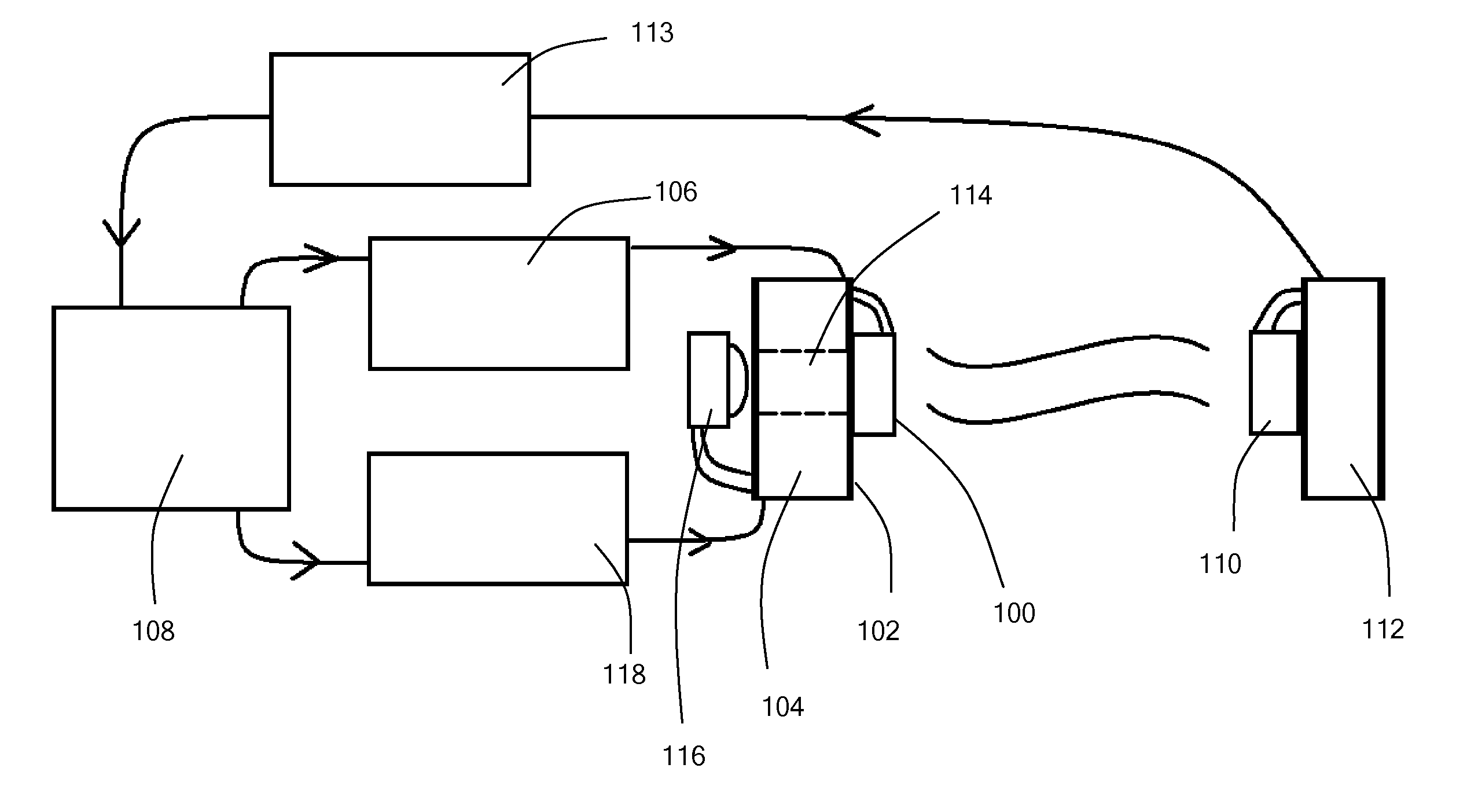
[0113]With reference to FIG. 6, a first indium aluminium antimonide light emitting diode 100, which emits radiation with a peak intensity at around 4.3 μm in use, is provided on a first side 102 of a 1.6 mm thick fibreglass resin printed circuit board 104. The first light emitting diode is formed according to EP 0 864 180, EP 0 992 094, and in Haigh, M. K. et al., Applied Physics Letters, vol. 90, 231116 (2007). This first light emitting diode is driven by an electronic circuit 106, under control of a microcontroller 108 to provide electromagnetic radiation which is detected by a photodiode 110. The photodiode is also based on indium aluminium antimonide and is mounted to a printed circuit board 112 which, when used with the gas sensor of FIGS. 1 to 5, is preferably a region of the printed circuit board to which the first light emitting diode is mounted, adjacent the light emitting diode, to facilitate thermal communication between the light emitting diode and the photodiode through...

example 2

[0119]In a second, alternative approach for obtaining a reference measurement, we have found that an indium aluminium antimonide based photodiode will emit light when driven using a conventional light emitting diode driving circuit. Similarly, an indium aluminium antimonide-based light emitting diode according to EP 0 864 180, EP 0 992 094, and in Haigh, M. K. et al., Applied Physics Letters, vol. 90, 231116 (2007), referred to above, can be used as a photodiode by attachment to a conventional photodiode amplifier circuit.

[0120]Thus, in the second example, a light emitting diode is pulsed, as before, and the current at the photodiode is measured to provide a measurement signal. Between each pulse of the light emitting diode, the photodiode is driven to emit radiation, and radiation received at the light emitting diode is measured using an amplifier. In this mode, the radiation emitted by the photodiode is predominantly at a significantly higher wavelength than the radiation emitted ...


PUM

PropertyMeasurementUnit
Fractionaaaaaaaaaa
Angleaaaaaaaaaa
Angleaaaaaaaaaa

Abstract

An optical absorption gas sensor includes a radiation source, detector and a radiation guide. The radiation source and detector are close together and in thermal communication. The radiation guide has a rectangular cross section and curves in a first sense, around an axis parallel to the major dimension of the rectangular cross section, and then in a second opposite sense, and again in the first sense. A relatively long path for radiation is provided in a compact device, without the attenuation of radiation which would occur if the radiation guide did not have a rectangular cross section and curved only around an axis parallel to the major dimension of the rectangular cross section. A reference measurement can be obtained by mounting a reference radiation source behind a translucent measurement radiation source and directing radiation from the reference radiation source through the measurement radiation source. Radiation from a reference radiation source may be directed around the measurement reference source. Measurement and reference signals can be obtained by using a light emitting diode to generate radiation which is detected by a photodiode, in a first operating mode, and driving the photodiode to generate radiation having a different emission spectrum while detecting the resulting radiation using the light emitting diode, in a second operating mode. An optical absorption gas sensor may be manufactured by abutting two or more L-shaped radiation guide portions to form a radiation guide. The radiation guide has an interior surface operable to reflect radiation emitted by the radiation source of the optical absorption gas sensor.

Description

FIELD OF THE INVENTION[0001]The invention relates to the field of optical absorption gas sensors, including but not limited to infra-red absorption gas sensors.BACKGROUND TO THE INVENTION[0002]Gas sensors are commonly employed in industrial and consumer applications to measure analytes in the gaseous state. Many gas sensors rely on the absorption characteristics of the target analyte when illuminated with radiation and comprise a radiation source, a detector capable of detecting radiation emitted by the radiation source, and a chamber for receiving the target gaseous analyte. Analyte gas within the chamber absorbs radiation of specific wavelengths or ranges of wavelengths and the attenuation of the radiation detected by the detector gives an indication of the concentration of the target analyte within the chamber. The target analyte typically diffuses into the chamber although sensors which actively transport gas into the chamber are known. In some optical absorption gas sensors, th...

Claims


Application Information

Patent Timeline
IPC IPC(8): G01N21/35B32B37/00
CPCG01N21/031Y10T156/10G01N2201/0636G01N21/3504
Inventor GIBSON, DESMOND ROBERTMACGREGOR, CALUM JOHNWADDELL, EWAN MACKINNON
Owner GAS SENSING SOLUTIONS
Why Eureka
Try Eureka