

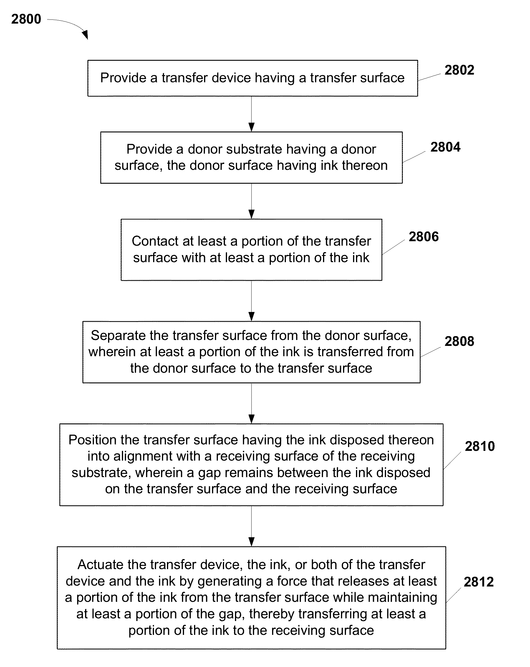
Non-contact transfer printing
a technology of non-contact transfer and printing press, which is applied in the direction of printing press, duplicating/marking method, printing, etc., can solve the problems of time- and material-related expenses of the process, and the risk of contamination of the final product, so as to avoid damage to the functional device
- Summary
- Abstract
- Description
- Claims
- Application Information
AI Technical Summary
Benefits of technology
Problems solved by technology
Method used
Image

Examples
example 1
Laser-Driven Non-Contact Transfer Printing (LNTP)
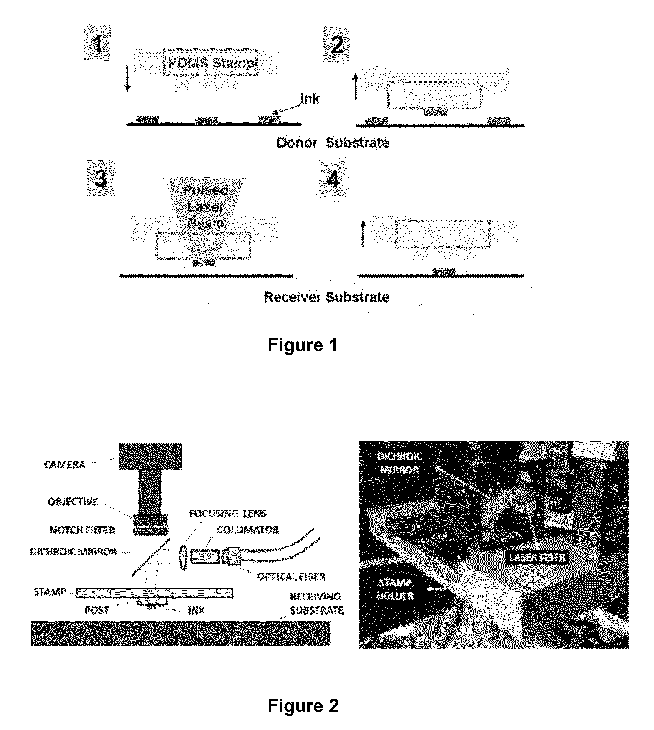
[0095]Mietl [10] describes a transfer printing process involving both the pick-up of microstructures from a donor substrate and their deposition or ‘printing’ onto a receiving substrate using an elastomeric stamp. The present invention also starts with an elastomeric stamp made of PDMS and optionally patterned with posts, to selectively engage the desired nano- or micro-devices on the donor or inking substrate. The mechanism for inking the stamp is similar to previously described mechanisms [4-8], relying on the strong adhesive forces between PDMS and the nano- or micro-devices to extract the ink from the donor or inking substrate. For deposition, however, the inked stamp is brought close (between 3 to 10 microns) to the receiving substrate onto which the devices are to be deposited. A pulsed laser beam is focused on the interface between the stamp and the devices to release and drive the device to the receiving substrate. The wavelen...
example 2
Laser-Driven Non-Contact Transfer Printing (LNTP) Onto Liquid Substrates
[0135]The LNTP process of the present invention can be used to transfer micro- or nano-devices (ink) to receiving substrates having various surface characteristics because the LNTP process is independent of receiving surface characteristics. For example, the receiving surface may be planar, rough, charged, neutral, non-planar, and / or contoured.
[0136]The present example demonstrates the applicability of the LNTP methods to liquids, biological cells, and the like. In the present example, a glass-backed transfer stamp having a 100 μm PDMS post was used to transfer a 3 μm thick×100 μm×100 μm silicon chip onto a water droplet disposed on a hydrophobic gold coating. The hydrophobicity of the gold coating causes the water droplet to present a highly spherical surface for receiving the silicon chip. A schematic of the technique is shown in FIG. 12(a) and a photograph of the silicon chip after transfer to the surface of ...
example 3
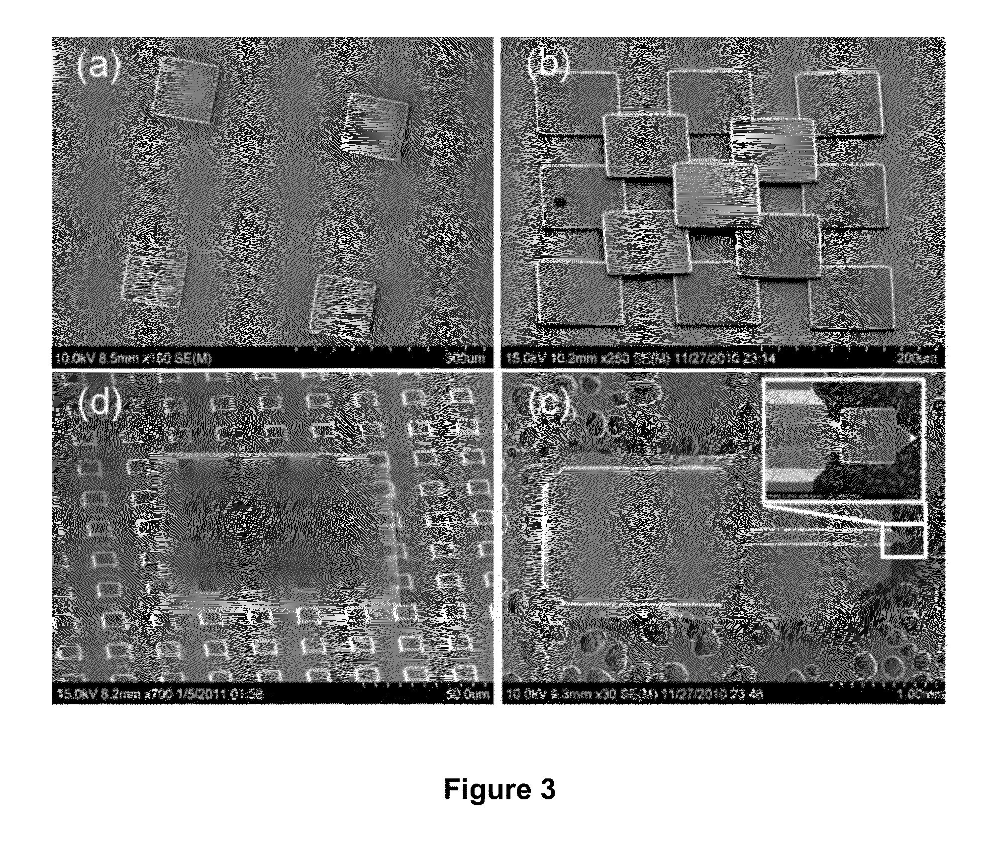
A Prototype Printer for Laser Driven Micro-Transfer Printing
[0137]This Example demonstrates a new mode of automated micro transfer printing called laser micro transfer printing (LμTP). As a process, micro-transfer printing provides a unique and critical manufacturing route to extracting active microstructures from growth substrates and deterministically assembling them into or onto a variety of functional substrates ranging from polymers to glasses and ceramics and metallic foils to support applications such as flexible, large-area electronics, concentrating photovoltaics and displays. Laser transfer printing extends micro-transfer printing technology by providing a non-contact approach that is insensitive to the preparation and properties of the receiving substrate. It does so by exploiting the difference in the thermo-mechanical responses of the microstructure and transfer printing stamp materials to drive the release of the microstructure or ‘ink’ from the stamp and its transfer ...
PUM
| Property | Measurement | Unit |
|---|---|---|
| Temperature | aaaaa | aaaaa |
| Temperature | aaaaa | aaaaa |
| Time | aaaaa | aaaaa |
Abstract
Description
Claims
Application Information