Magnetic tunnel junction for MRAM applications
a tunnel junction and magnetic tunnel junction technology, applied in the direction of magnets, galvano-magnetic material selection, inductance/transformer/magnet manufacturing, etc., can solve the problems of poor writing margin, inability to directly apply structure in mram, and deformation in one or more other parameters, so as to improve the reading margin, improve the mr ratio, and improve the effect of mr ratio
- Summary
- Abstract
- Description
- Claims
- Application Information
AI Technical Summary
Benefits of technology
Problems solved by technology
Method used
Image
Examples
first embodiment
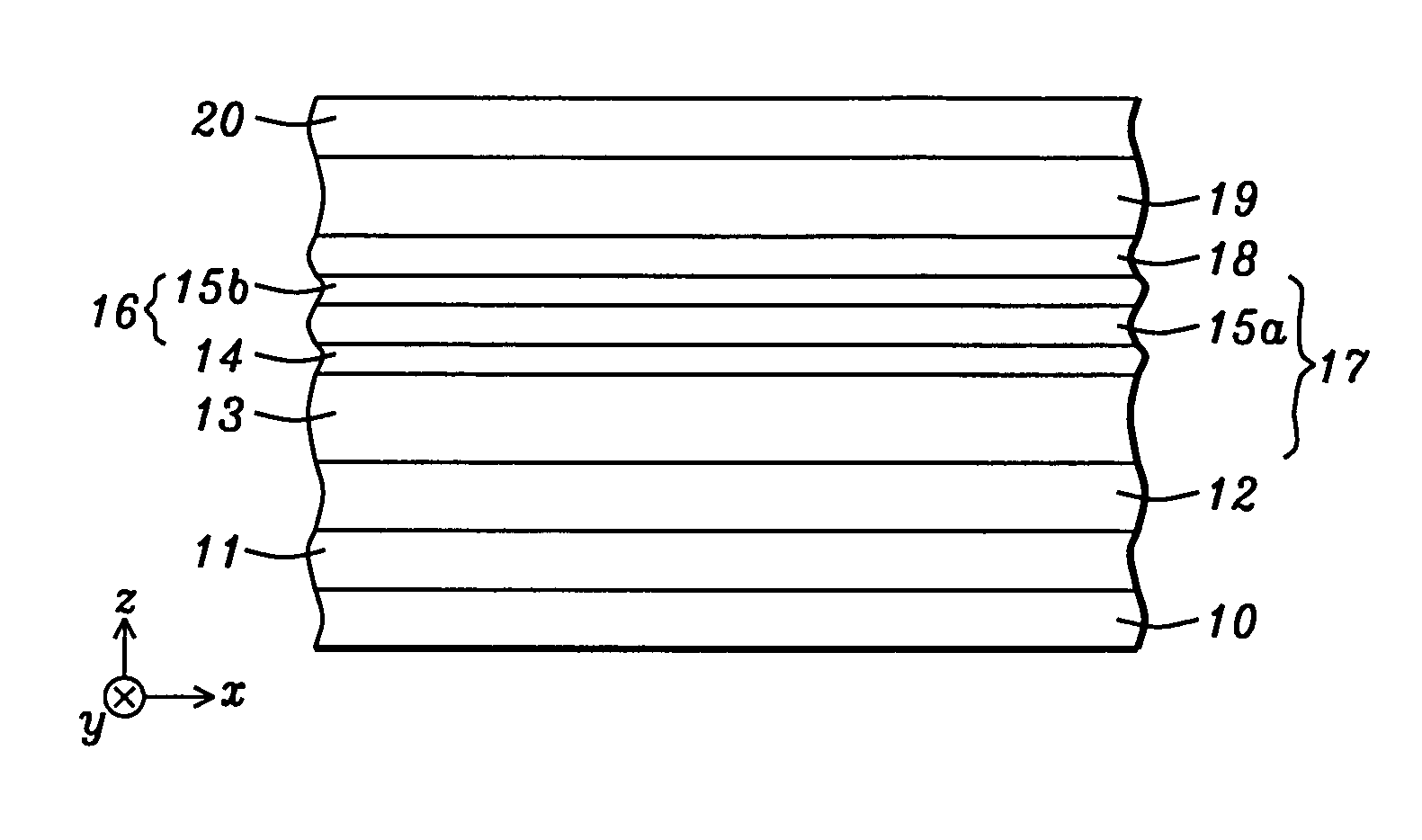
[0030]Referring to FIG. 1, a MTJ structure is illustrated according to the present invention. The substrate 10 may be a bottom conductor layer, for example, also known as a bottom electrode and having a thickness in the z-axis direction and with a top surface in the x,y plane. A MTJ stack of layers is now formed on the substrate 10. It should be understood that all layers in the MTJ stack may be formed in the same process tool such as an Anelva C-7100 thin film sputtering system or the like which typically includes three physical vapor deposition (PVD) chambers, an oxidation chamber, and a sputter etching chamber. At least one of the PVD chambers is capable of co-sputtering using two or more targets. Typically, the sputter deposition process involves an argon sputter gas and the targets are made of metal or alloys to be deposited on a substrate. All MTJ layers may be formed after a single pump down of the sputter system to enhance throughput.
[0031]In the exemplary embodiment depicti...
second embodiment
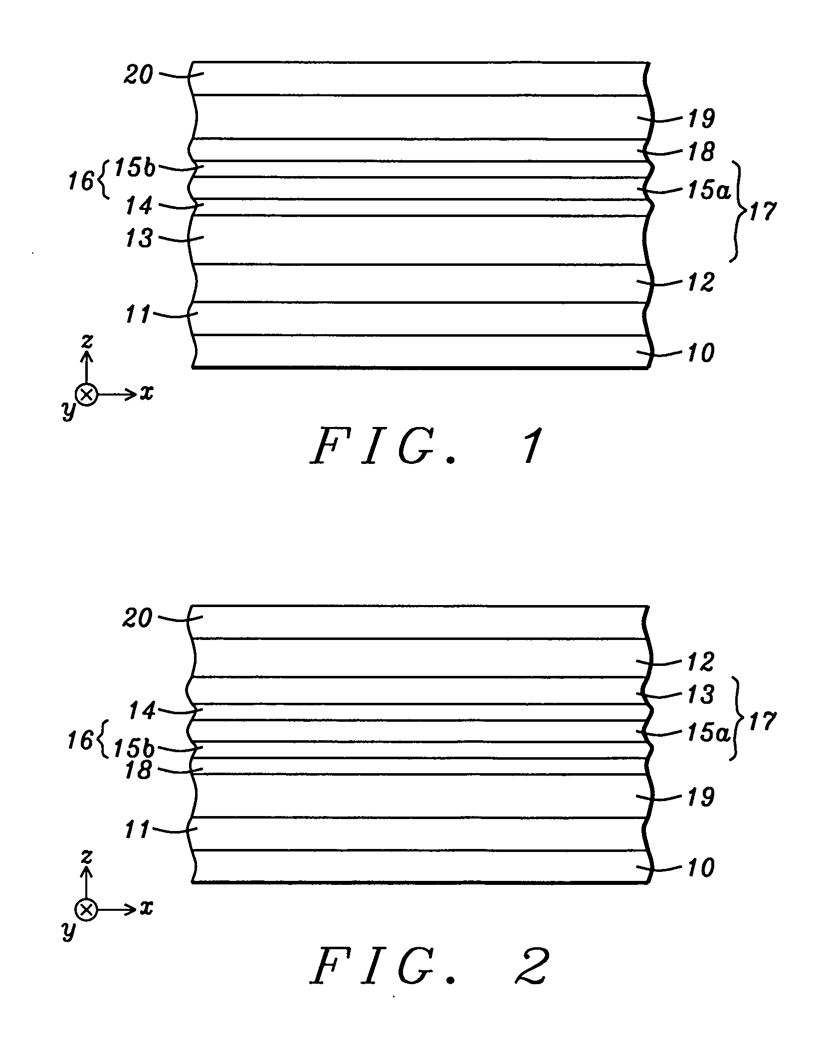
[0048]According to the present invention as depicted in FIG. 2, the free layer 19 as described in the bottom spin valve embodiments may be formed in a top spin valve configuration. For example, the MTJ stack may be fabricated by sequentially forming a seed layer 11, composite free layer 19, tunnel barrier 18, SAF pinned layer 17, AFM layer 12, and capping layer 20 on substrate 10. In this case, free layer 19 may have a FL2 / FL1 (NiFeX / Fe) or a FL3 / FL2 / FL1 (NiFeX / Fe / CoFe) configuration wherein the NiFeX layer is the bottom layer in the free layer stack and contacts a top surface of seed layer 11. Thus, the uppermost FL1 layer interfaces with the tunnel barrier 18 to produce a high MR ratio. The properties and thicknesses of the aforementioned layers are retained from the previous embodiments. Note that the SAF pinned layer 17 has an AP1 / coupling / AP2 configuration wherein the AP1 layer 16 contacts a top surface of the tunnel barrier layer and the AP2 layer 13 contacts a bottom surface ...
PUM
 Abstract
Description
Claims
Application Information


