Method for producing thin-film light-absorbing layer and method for manufacturing thin-film solar cell including the same

a solar cell and light-absorbing layer technology, applied in the field of producing thin-film light-absorbing layer and manufacturing thin-film solar cells including the same, can solve the problems of high manufacturing cost, long processing time, and high photoelectric conversion efficiency of silicon solar cells, and achieve high photoelectric conversion efficiency and cost reduction

Active Publication Date: 2013-02-28
KOREA INST OF SCI & TECH
View PDF2 Cites 13 Cited by
  • Summary
  • Abstract
  • Description
  • Claims
  • Application Information

AI Technical Summary

Benefits of technology

[0017]It is an object of the present invention to provide a method for producing a highly dense CIGS thin film from the CIGS powder precursors or a paste or an ink including the powder precursors by a non-vacuum process in a simple, highly reliable and economical manner.
[0024]In the method of the present invention, the thickness of the powder coat layer may be reduced by 50 to 90% of its original thickness with additional compressioning to improve the particle packing density of the powder coat layer.
[0033]The methods of the present invention use a powder process of non-vacuum processes to produce a copper indium selenium (CIS) or copper indium gallium selenium (CIGS) thin-film light-absorbing layer. According to the methods of the present invention, a very dense thin film of CIS or CIGS can be produced even by the low-temperature sintering. Therefore, these thin films enable the manufacture of a thin-film solar cells of CIS or CIGS with high photoelectric conversion efficiency at reduced cost.

Problems solved by technology
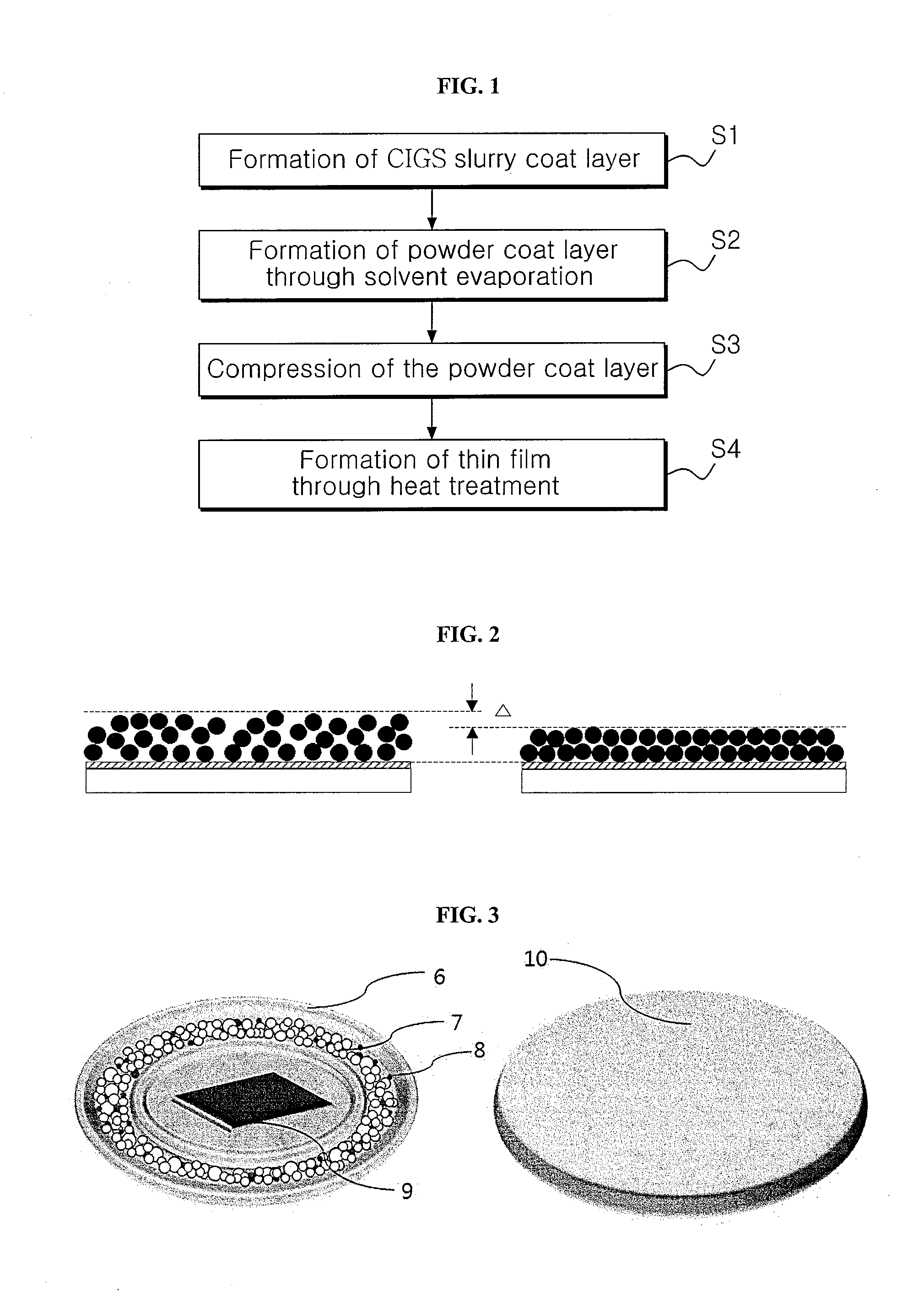
However, only a few solar cells using inorganic and organic semiconductors have been commercially successful to date, and typical examples thereof are silicon (Si) solar cells, copper indium selenium (CIS) solar cells and copper indium gallium selenium (CIGS) solar cells.
Silicon solar cells exhibit high photoelectric conversion efficiency but have the disadvantage of high manufacturing costs.
On the other hand, it has drawbacks as follows: long processing time, high materials loss up to 20-40%, and very complicated process control due to multicomponent systems of three or four components.
However, it is not easy to produce a dense CIGS light-absorbing layer by a powder method from the powder precursors or a paste or an ink including the powder precursors.
In order to obtain a dense film without open pores penetrating the film by a powder process, either thick powder coats or sintering at high temperature are inevitably chosen, which causes detrimental effects of high material loss or thermal damage of the substrate.

Method used


Image

  • Method for producing thin-film light-absorbing layer and method for manufacturing thin-film solar cell including the same
  • Method for producing thin-film light-absorbing layer and method for manufacturing thin-film solar cell including the same
  • Method for producing thin-film light-absorbing layer and method for manufacturing thin-film solar cell including the same

Examples


example 1

[0088]1) Preparation of CIGS Compound Powder

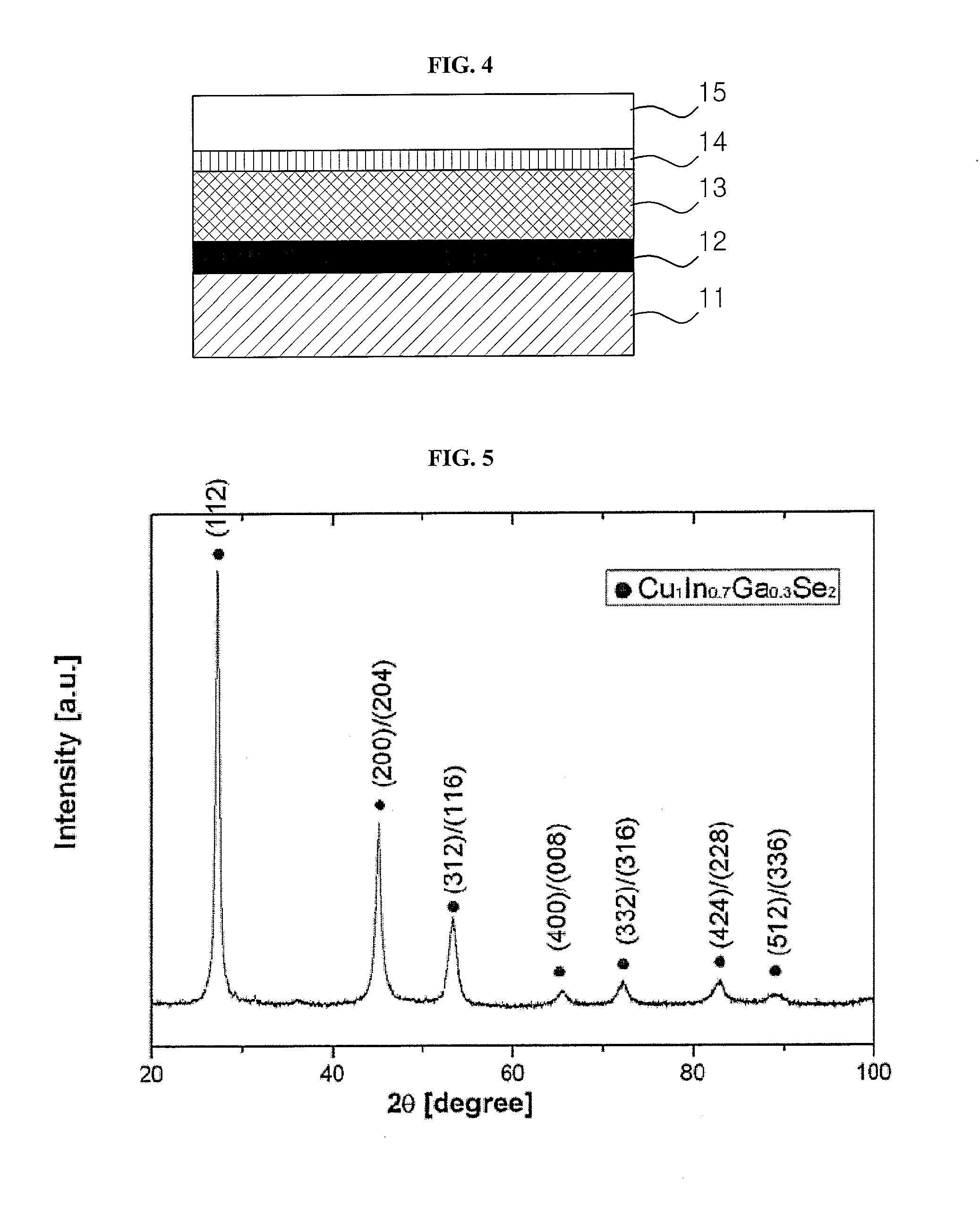
[0089]A copper metal powder (Cu purity 99.9%, average diameter 140 μm), an indium metal powder (In purity 99.99%, average diameter 140 μm), a gallium metal powder (Ga purity 99.99%, liquid at room temperature) and a selenium powder (Se purity 99.99%, average diameter 140 μm) as raw materials were mixed to compose CuInxGa1-xSey (x=0.7, y=2). The mixture was placed in a stainless steel jar filled with zirconia balls and dry milled in a planetary milling machine at 200 rpm for 30 min. X-ray diffraction and scanning electron microscopy (SEM) analysis indicated that the mixture had a single phase of the composition CuInxGa1-xSey (x=0.7, y=2) and was polydispersed in size having an average diameter of 30 to 850 nm. The diffraction results are shown in FIG. 5 and a SEM image of the mixture is shown in FIG. 6.

[0090]2) Preparation of the Powder Slurry

[0091]Pentanol (95.5 wt %), ethyl cellulose (3.0 wt %) and a powder dispersant (KD-2) (1.5 wt %) we...

example 2

[0100]A thin film was produced in the same manner as in Example 1 from step 1) to 4), but step 5) for thin-film formation follows the method explained in Example 2 instead.

[0101]The alumina powder (Al2O3 purity 99.8%, average particle size 75 μm), heat treated at 250° C. for 1 hr, was mixed with a selenium powder (Se purity 99.99%, average diameter 140 μm) in a weight ratio of 4:1. For homogeneous mixing of the selenium and alumina powders, the powder mixture was ball-milled in a 250 ml Nalgene bottle filled with 5-mm zirconia balls at 140 rpm for 2 hr. During the ball milling, the atmosphere was charged with argon to protect the powder mixture from air oxidation. The selenium powder may be in different size after the ball milling.

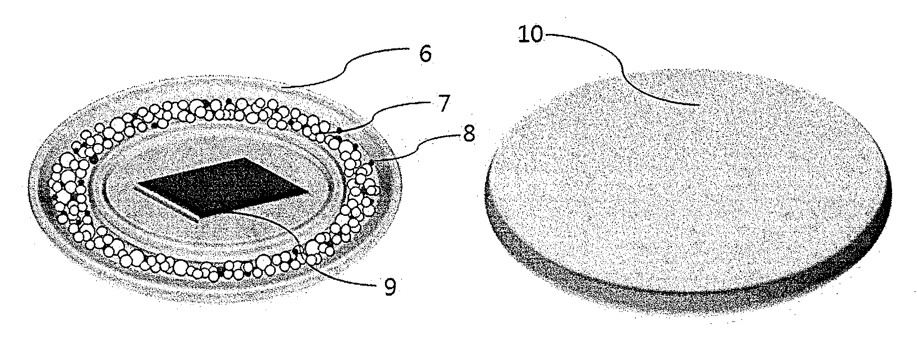
[0102]As illustrated in FIG. 3, the substrate 9, on which the CIGS powder layer with improved packing density is formed, was placed in an alumina crucible 6, and then 0.5 g of the ball-milled powder mixture of alumina 7 and selenium 8 was placed around the...

experimental example 1

Comparison of Electrical Properties

[0105]The electrical properties of the thin film produced by selenization after compression in Example 2 were compared with those of the thin film produced by selenization without compression in Comparative Example 2. The electrical properties of a thin film have a direct influence on the efficiency of a thin-film solar cell. That is, high electron mobility and electrical conductivity of a thin film may lead to high efficiency of a solar cell. The electrical properties of the thin films produced in Example 2 and Comparative Example 2 were measured using a Hall effect measurement system (Ecopia HMS3000) at a magnetic field of 0.57 T by the Van der Pauw method. A 4-point probe method was used to analyze the CIGS thin films deposited on the glass substrates.

TABLE 1BulkMobilityConductivityconcentrationμResistivityσp (cm−3)(cm2 / Vs)p (Ω· cm)(1 / Ω· cm)(a) Example 28.6 × 10167.21.00.10(b) Comparative9.2 × 10160.641060.0094Example 2(c) Example 11.4 × 10170.4...


PUM

PropertyMeasurementUnit
pressureaaaaaaaaaa
band gap energyaaaaaaaaaa
thicknessaaaaaaaaaa

Abstract

Disclosed is a method for producing a copper indium selenium (CIS) or copper indium gallium selenium (CIGS) thin-film light-absorbing layer. The method includes forming a coating layer of CIGS slurry, removing a solvent, a dispersant and a binder from the coating layer to form a powder coat layer, pressing the powder coat layer to improve its particle packing density, and heating the powder layer to form a dense thin film. The method uses a powder process as a non-vacuum process to produce a CIS or CIGS thin film in high yield at low cost. Further disclosed is a method for manufacturing a thin-film solar cell including the production method.

Description

CROSS-REFERENCE TO RELATED APPLICATIONS[0001]This application claims priority under 35 U.S.C. §119 to Korean Patent Applications No. 10-2011-0083444 filed on Aug. 22, 2011 in the Korean Intellectual Property Office, the disclosure of which is incorporated herein by reference in its entirety.BACKGROUND OF THE INVENTION[0002]1. Field of the Invention[0003]The present invention relates to a method for producing a copper indium selenium (CIS) or copper indium gallium selenium (CIGS) thin-film light-absorbing layer that can be applied to a thin-film solar cell, and a method for manufacturing a thin-film solar cell including the same.[0004]2. Description of the Related Art[0005]Solar cells are the devices that directly converts light energy into electrical energy. Solar cells have received the most intensive attention as potential systems for future energy production due to their ability to safely produce clean energy from the vast sunlight. Various kinds of inorganic and organic semicond...

Claims


Application Information

Patent Timeline
Patent Type & Authority Applications(United States)
IPC IPC(8): H01L31/0264B05D5/06B05D3/02H01L31/18
CPCH01L31/0322Y02E10/541Y02P70/50H01L31/0445H01L31/0216H01L31/18
Inventor CHO, SO HYEPARK, JONG KUSONG, BONG GEUNKIM, KYUNGHOONPARK, HYUNG HO
Owner KOREA INST OF SCI & TECH
Why Eureka
Try Eureka