Multi-working voltages CMOS device with single gate oxide layer thickness and manufacturing method thereof

a technology of multi-working voltage and cmos, which is applied in the direction of semiconductor devices, electrical devices, transistors, etc., can solve the problems of increased preparing cost of semiconductor devices and difficult preparation processes, and achieve low preparation cost, convenient to execute, and suitable for industrial production

Inactive Publication Date: 2013-02-28
SHANGHAI HUALI MICROELECTRONICS CORP
View PDF0 Cites 14 Cited by
  • Summary
  • Abstract
  • Description
  • Claims
  • Application Information

AI Technical Summary

Benefits of technology

[0035]The multi-working voltages CMOS device with single gate oxide layer thickness of the present invention regulates a gate work function of CMOS transistors by implanting ions with different work functions into a metal oxide dielectric material layer of the CMOS transistors, to realize different flat-band voltages under the condition of single dielectric layer thickness, and to realize multi-working voltages CMOS structure under the condition of single dielectric layer thickness. The manufacturing process of the present invention is simple and easy

Problems solved by technology

However, in the above method which changes the gate dielectric layer thicknesses of the MOS transistors to regulate threshold voltages of the MOS transistors so as to realize multi-working voltages of the semiconductor device, the preparing processes of

Method used


Image

  • Multi-working voltages CMOS device with single gate oxide layer thickness and manufacturing method thereof
  • Multi-working voltages CMOS device with single gate oxide layer thickness and manufacturing method thereof
  • Multi-working voltages CMOS device with single gate oxide layer thickness and manufacturing method thereof

Examples


first embodiment

[0091]Hereinafter, the first embodiment of the present invention will be described with reference to FIG. 4 to FIG. 9.

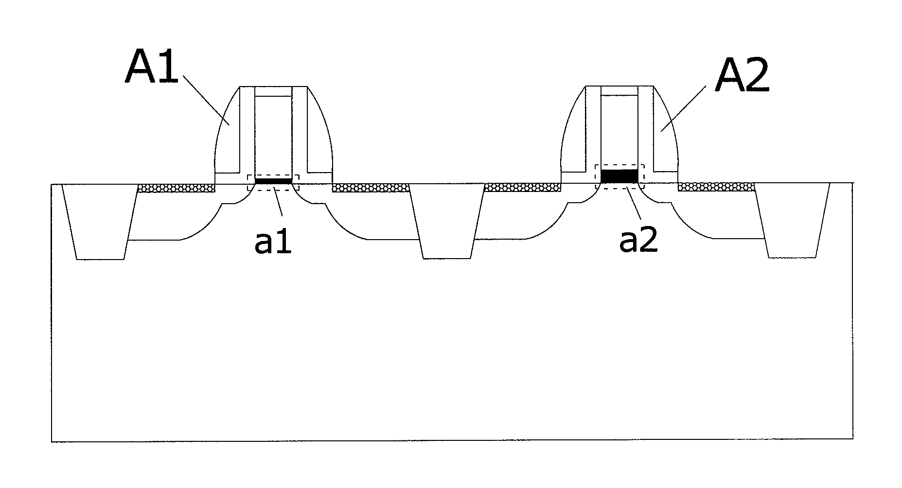
[0092]According to the first embodiment, the present invention provides a multi-working voltages CMOS device with single gate oxide layer thickness, which comprises a plurality of N-type and P-type MOS transistors, a gate of each of the N-type and P-type MOS transistors comprises a metal oxide dielectric material layer with same thickness; and work functions of the MOS transistors are regulated by implanting ions into the metal oxide dielectric material layers of the MOS transistors; the change of work functions realizes different flat-band voltages under the condition of single dielectric layer (here, i.e., a metal oxide dielectric material layer) thickness, so as to change the working voltages of the MOS devices, thus to realize multi-working voltages CMOS structure under the condition of single dielectric layer thickness.

[0093]As shown in FIG. 4, it is a dual-work...

second embodiment

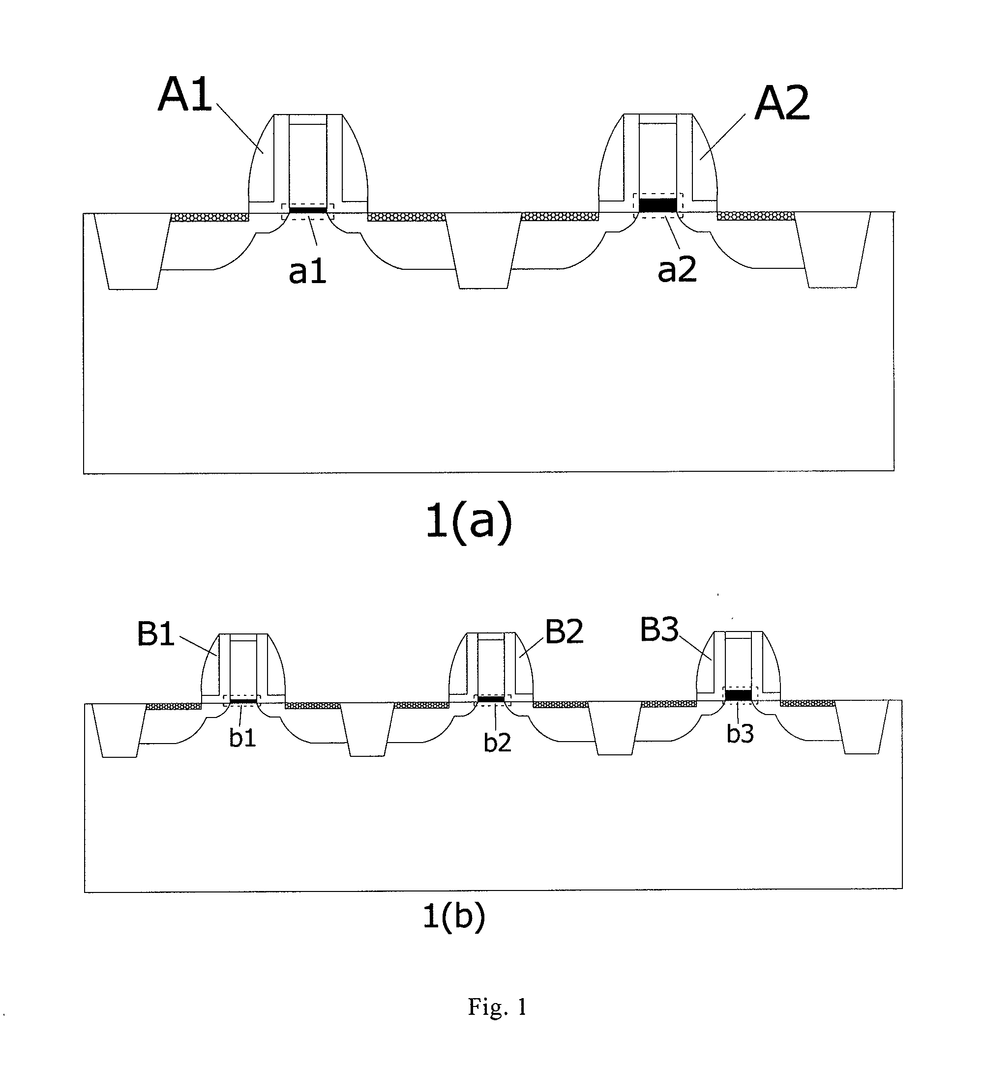
[0116]The second embodiment of the present invention is described below with reference to FIG. 10 to FIG. 14.

[0117]The first type transistors and second type transistors referred to in the second embodiment of the present invention indicate pairs of PMOS transistors and NMOS transistors, but the first type transistors of the present invention do not indicate PMOS transistors specifically, those skilled in the art can determine the first type transistors and the second type transistors according to specific situations, which will not be described unnecessarily herein.

[0118]Referring to FIG. 3 again, different flat-band voltages can be realized by changing the work functions of Poly-Silicon or metal layers, so as to realize Multi-working voltages of CMOS under the condition of single dielectric layer thickness.

[0119]The second embodiment of the present invention uses this principle to realize multi-working voltages CMOS structure with single gate oxide layer thickness. Please refer to...


PUM


Abstract

The present invention provides a multi-working voltages CMOS device with single gate oxide layer thickness, gate work functions of CMOS transistors are regulated by implanting ions with different work functions into metal oxide dielectric material layers of the CMOS transistors, thus to realize different flat-band voltages under the condition of single dielectric layer thickness, and realize a multi-working voltages CMOS structure under the condition of single dielectric layer thickness. The present invention overcomes the process complexity of multiple kinds of gate dielectric layer thicknesses needed by traditional multi-working voltages CMOS, simplifies the CMOS process, makes the manufacturing procedure simple and easy to execute, reduces the preparation cost and is suitable for industrial production.

Description

CROSS REFERENCE TO RELATED APPLICATIONS[0001]The present application is based upon and claims priority under 35 U.S.C. §119 to prior Chinese Patent Application No. 201110265327.8 filed on Sep. 8, 2011 and prior Chinese Patent Application No. 201110250267.2 filed on Aug. 29, 2011, the entire contents of which are incorporated herein by reference.FIELD OF THE INVENTION[0002]The present invention relates to a manufacturing method of an integrated circuit, and particularly to a multi-working voltages CMOS device with single gate oxide (GOX) layer thickness and a manufacturing method thereof, and a multi-working voltages gate-last process semiconductor device with single gate oxide layer thickness and a manufacturing method thereof.BACKGROUND OF THE INVENTION[0003]In logic circuits or memory circuits of semiconductors, multi-working voltages are adopted in many CMOS (Complementary Metal-Oxide-Semiconductors) because of requirements for circuit design.[0004]For example, working voltages f...

Claims


Application Information

Patent Timeline
IPC IPC(8): H01L27/092H01L27/12H01L21/86H01L21/8238
CPCH01L21/823857
Inventor HUANG, XIAOLUMAO, GANGCHEN, YUWENXIE, XINYUN
Owner SHANGHAI HUALI MICROELECTRONICS CORP
Why Eureka
Try Eureka