Antenna device

Active Publication Date: 2013-02-28
ORMON CORP
View PDF1 Cites 18 Cited by
  • Summary
  • Abstract
  • Description
  • Claims
  • Application Information

AI Technical Summary

Benefits of technology

[0018]In the antenna device of an aspect of the invention, in consideration of this problem, the inner conductor of the coaxial cable and the feed pin are connected in series through an impedance converting capacitor. The reactance or resistance component of the feed pin is cancelled by the capacitor, and the impedance of the RF-signal route in the antenna board can be matched with the impedance of the coaxial cable. Therefore, the gain can be enhanced by the thickness of the board without degrading the radiation efficiency.
[0019]According to the inventi

Problems solved by technology

In the antenna device disclosed in Japanese Unexamined Patent Publication No. 2004-72320, the circuit board is disposed in the shie

Method used


Image

  • Antenna device
  • Antenna device
  • Antenna device

Examples


Embodiment Construction

[0026]Embodiments of a compact antenna device according to the invention will be described with reference to FIGS. 1A to 4. Identical elements shown in the various figures are designated with the same reference numerals.

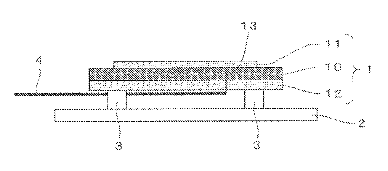
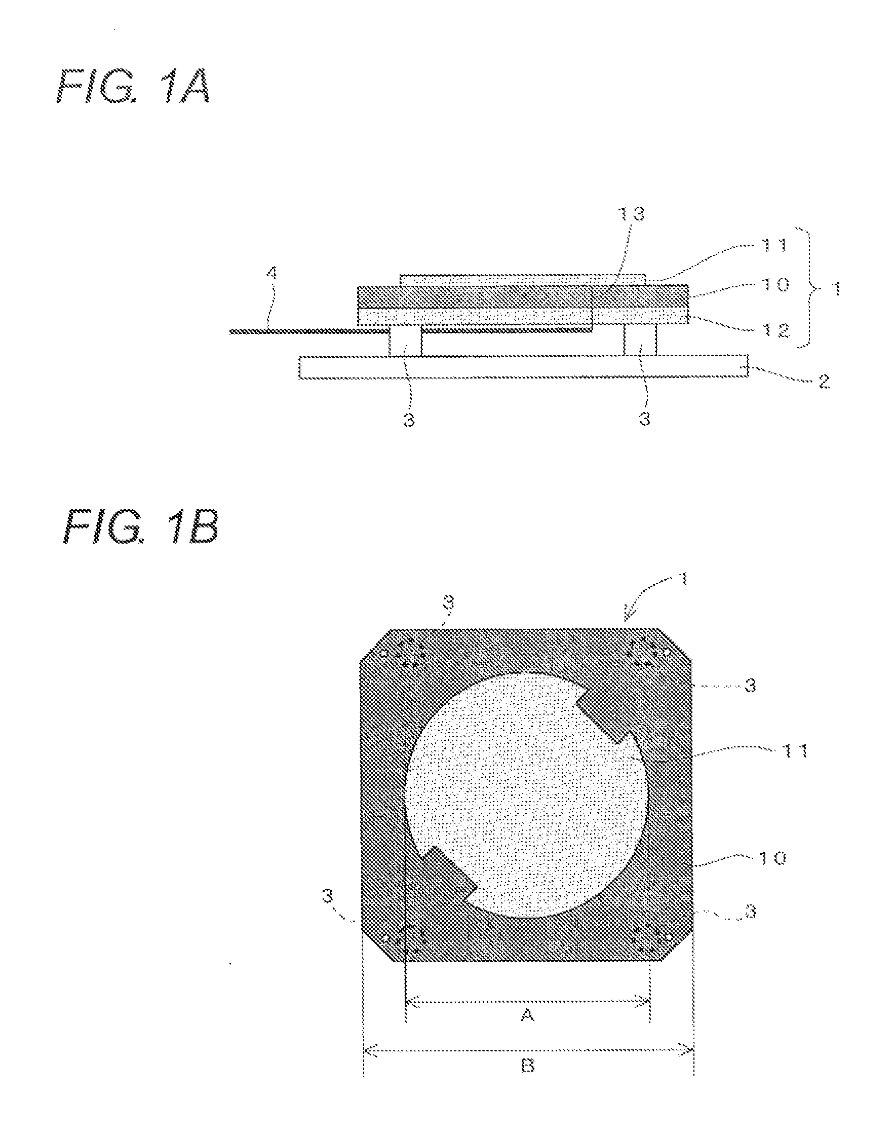
[0027]FIGS. 1A and 1B each illustrate a configuration of a main part of an RFID-system antenna device according to an embodiment of the invention. FIG. 1A is a side view of the main part, and FIG. 1B is a front view of the main part.

[0028]The main part of the antenna device of the embodiment comprises a coupled body of an antenna board 1 and a metallic plate 2. In a configuration of the antenna board 1, front-surface-side conductive layer 11 and rear-surface-side conductive layer 12 are formed in or on both surfaces of a square dielectric plate 10, in which the four corners are cut off. The front-surface-side conductive layer 11 has a circular shape, in which two arcs disposed opposite each other are notched, and acts as an antenna pattern. The rear-surface-side cond...


PUM


Abstract

An antenna device comprises an antenna board, wherein an antenna pattern is formed in or on a front surface of a dielectric layer, a ground layer is formed in or on a rear surface of the dielectric layer, and a feed pin is inserted into a thickness of the antenna board through the ground layer and the dielectic layer. The diameter of the antenna pattern is set to one half of the wavelength of an RF signal passed through the antenna pattern, and a length of one side of the dielectric plate is set shorter than the wavelength. A metallic plate is coupled to the ground layer with a plurality of metallic spacers interposed therebetween, whereby the metallic plate is electrically connected to the ground layer. .

Description

TECHNICAL FIELD[0001]The present invention relates to a radio-communication antenna device, particularly to an antenna device comprising a configuration of a patch antenna.RELATED ART[0002]In a configuration of an antenna board for a patch antenna, a conductive layer that acts as an antenna pattern is formed in or on one of the surfaces of a dielectric plate, and a ground layer is formed in or on the other surface. The antenna pattern is electrically connected to a feed pin that is inserted into a middle substrate of the antenna board, and the feed pin is electrically connected to a coaxial cable that transmits a radio frequency (RF) signal. When the RF signal from the coaxial cable is supplied to the antenna pattern through the feed pin, an electric field is generated between the antenna pattern and the ground layer to radiate a radio wave.[0003]Japanese Unexamined Patent Publication No. 4-337907 discloses a configuration of a basic antenna board. In the antenna board disclosed in ...

Claims


Application Information

Patent Timeline
IPC IPC(8): H01Q1/38
CPCH01Q1/38H01Q9/045H01Q9/0414H01Q1/48
Inventor NOGAMI, HIDEKATSU
Owner ORMON CORP
Why Eureka
Try Eureka