Graphene on Semiconductor Detector

a semiconductor detector and graphene technology, applied in the direction of diodes, semiconductor devices, radiation control devices, etc., can solve the problems of degrading the quantum efficiency of the imager especially at ultraviolet wavelengths, and achieve the effect of low sheet resistan

Inactive Publication Date: 2013-04-04
THE UNITED STATES OF AMERICA AS REPRESENTED BY THE SECRETARY OF THE NAVY
View PDF3 Cites 129 Cited by
  • Summary
  • Abstract
  • Description
  • Claims
  • Application Information

AI Technical Summary

Benefits of technology

[0003]Various details of the present disclosure are hereinafter summarized to facilitate a basic understanding, where this summary is not an extensive overview of the disclosure, and is intended neither to identify certain elements of the disclosure, nor to delineate the scope thereof. Rather, the primary purpose of this summary is to present some concepts of the disclosure in a simplified form prior to the more detailed description that is presented hereinafter.
[0004]Ultraviolet (UV) and/or Extreme Ultraviolet (EUV) wavelength photodetector and imager structures are disclosed in which a graphene electrode is used to collect photogenerated carriers and establish a potential on the surface of a semiconductor material. Backside illuminated detector and imagers are disclosed that have a thin backside graphene transparent conductive layer. A variety of types of photodetectors are possible, including without l

Problems solved by technology

Backside illuminated active pixel, hybrid, and charge coupled device imagers often have a dead layer on the backside that degrade the imager quantum efficiency especially at ultraviolet wavelengths.

Method used


Image

  • Graphene on Semiconductor Detector
  • Graphene on Semiconductor Detector
  • Graphene on Semiconductor Detector

Examples


Embodiment Construction

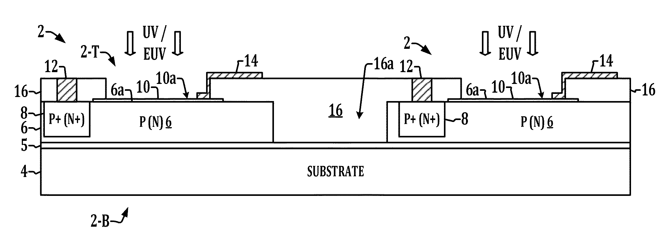
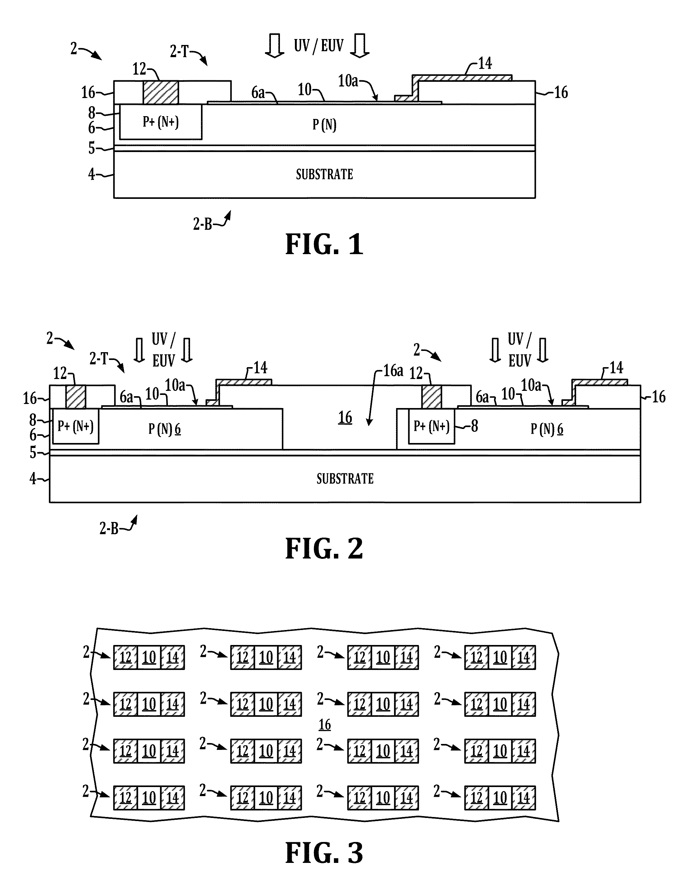
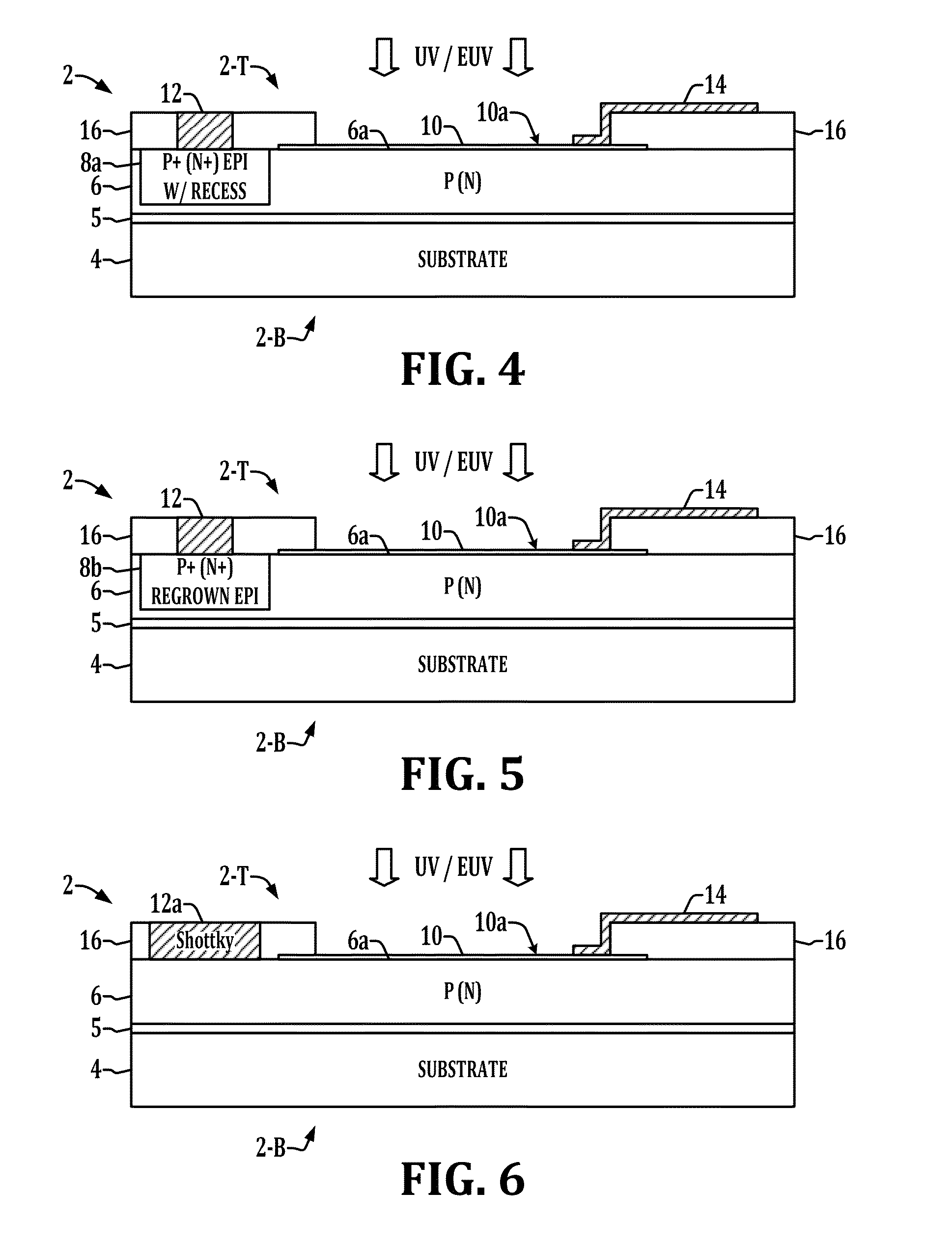
[0028]One or more embodiments or implementations are hereinafter described in conjunction with the drawings, where like reference numerals refer to like elements throughout, and where the various features are not necessarily drawn to scale.

[0029]Referring initially to FIGS. 1-10, several exemplary embodiments of a photodetector apparatus are disclosed which may include one or more photo detector cells 2, 32. The disclosed apparatus of these embodiments generally provides a semiconductor structure 6 with an upper surface 6a, along with a thin graphene layer 10 disposed over the upper surface 6a. Graphene is substantially an sp2 bonded carbon layer which is sometimes formed one or more two dimensional honeycomb crystal lattice layers or sheets with a carbon-carbon bond length of about 0.142 nm, where sheets may be stacked with an interplanar spacing of about 0.335 nm, and may be stacked in certain arrangements such as A-B ordering. In certain embodiments, a very thin graphene layer 10...


PUM


Abstract

Ultraviolet or Extreme Ultraviolet and/or visible detector apparatus and fabrication processes are presented, in which the detector includes a thin graphene electrode structure disposed over a semiconductor surface to provide establish a potential in the semiconductor material surface and to collect photogenerated carriers, with a first contact providing a top side or bottom side connection for the semiconductor structure and a second contact for connection to the graphene layer.

Description

REFERENCE TO RELATED APPLICATION[0001]This application claims priority to and the benefit of U.S. Provisional Patent Application Ser. No. 61 / 540,706, filed Sep. 29, 2011, and entitled “Graphene on Semiconductor UV or EUV Photodetector”, the entirety of which is hereby incorporated by reference into the present disclosure.BACKGROUND[0002]Photodetectors are used in a wide variety of applications to sense visible light and other electromagnetic radiation, such as for recording images in astronomy, digital photography, and digital cinematography, etc. Certain applications involve detection of Ultraviolet (UV) and / or Extreme Ultraviolet (EUV or XUV) radiation, where UV involves wavelengths from about 10 nm to 400 nm and is thus shorter than visible light but longer than X-rays, corresponding to photon energies from about 3 eV to 124 eV. EUV is often regarded as high-energy electromagnetic radiation having wavelengths in a range of about 10 nm to 120 nm involving photons with energies fro...

Claims


Application Information

Patent Timeline
IPC IPC(8): H01L27/148H01L31/0336
CPCH01L27/148H01L27/14643H01L31/028H01L27/14694H01L31/0336H01L27/14692
Inventor KUB, FRANCIS J.ANDERSON, TRAVISHOBART, KARL D.
Owner THE UNITED STATES OF AMERICA AS REPRESENTED BY THE SECRETARY OF THE NAVY
Why Eureka
Try Eureka