High Throughput Thin Film Characterization And Defect Detection

a thin film, defect detection technology, applied in the direction of optically investigating flaws/contamination, semiconductor/solid-state device testing/measurement, instruments, etc., can solve the problems of high cost and low throughput of x-ray spectroscopy, affecting chip performance at the end of the manufacturing process, and being unsuitable for use as a high throughput production monitoring tool

Active Publication Date: 2013-04-04
KLA TENCOR TECH CORP
View PDF7 Cites 30 Cited by
  • Summary
  • Abstract
  • Description
  • Claims
  • Application Information

AI Technical Summary

Benefits of technology

[0012]High throughput spectrometers such as ellipsometers or reflectometers quickly measure semiconductor wafers early in the manufacturing process. In addition, these optical tools are capable of gath

Problems solved by technology

This affects chip performance at the end of the manufacturing process.
However, X-ray spectroscopy suffers from high cost and low throughput, making it undesireable for use as a high throughput production monitoring tool.
The resulting structural defects or band structure may adversely increase leakage

Method used


Image

  • High Throughput Thin Film Characterization And Defect Detection
  • High Throughput Thin Film Characterization And Defect Detection
  • High Throughput Thin Film Characterization And Defect Detection

Examples


Embodiment Construction

[0025]Reference will now be made in detail to background examples and some embodiments of the invention, examples of which are illustrated in the accompanying drawings.

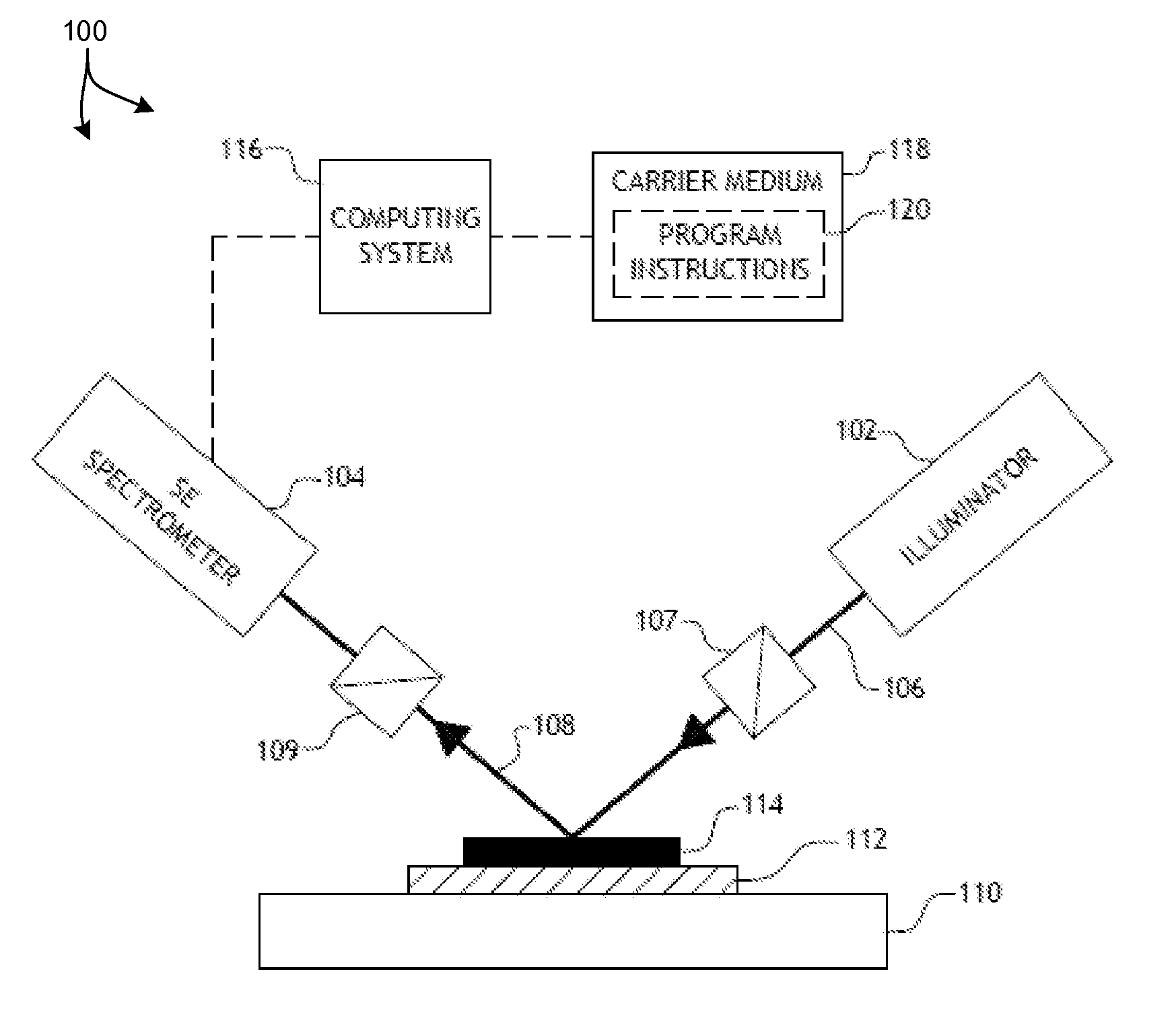
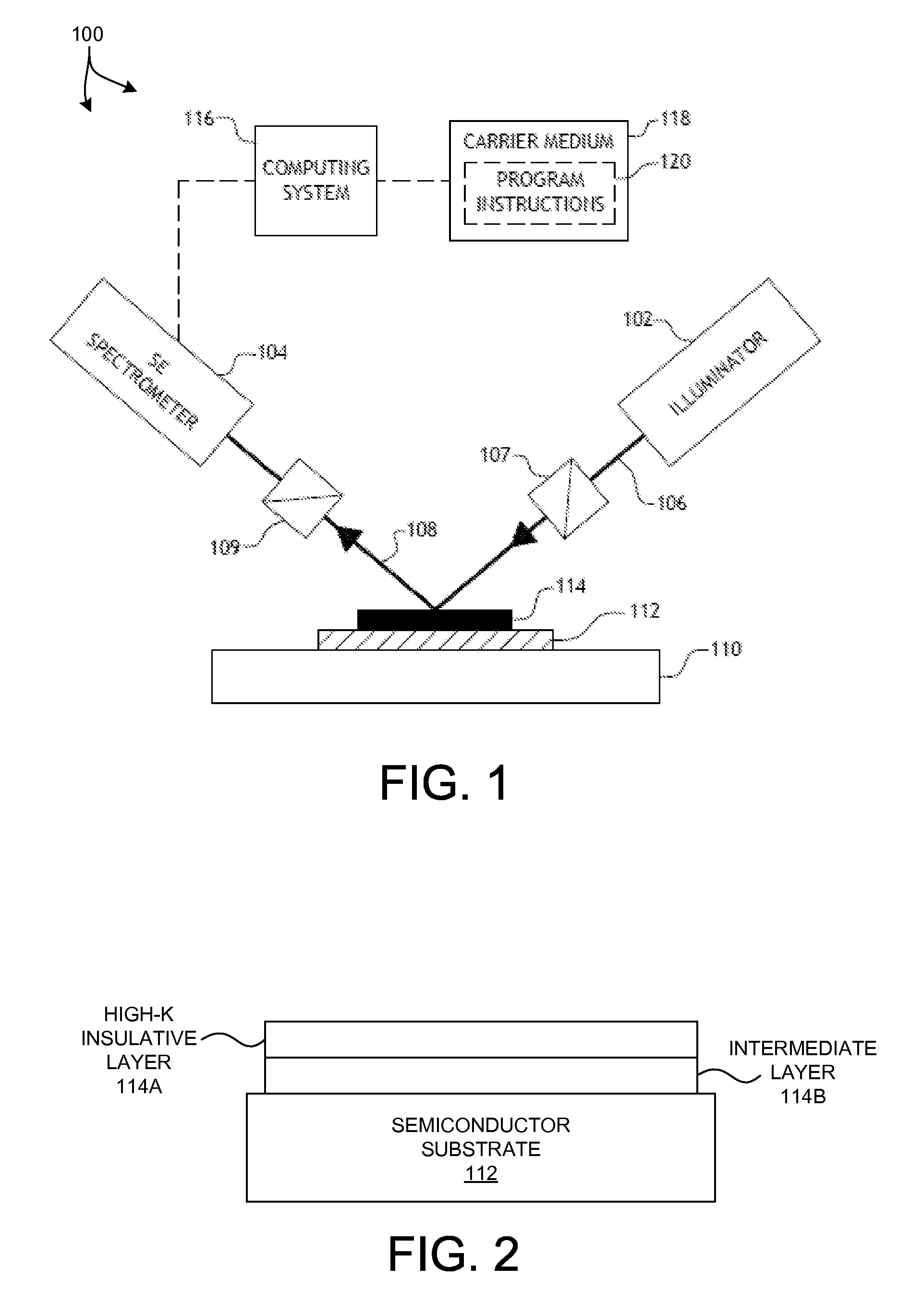
[0026]FIG. 1 illustrates a system 100 for measuring a band structure characteristic of a thin film of a semiconductor wafer, in accordance with one embodiment of the present invention. As shown in FIG. 1, the system 100 may be used to perform spectroscopic ellipsometry on one or more films 114 of a semiconductor wafer 112 disposed on a translation stage 110. In this aspect, the system 100 may include a spectroscopic ellipsometer equipped with an illuminator 102 and a spectrometer 104. The illuminator 102 of the system 100 is configured to generate and direct illumination of a selected wavelength range (e.g., 150-850 nm) to the thin film (e.g., HfSiON thin film) disposed on the surface of the semiconductor wafer 112. In turn, the spectrometer 104 is configured to receive illumination reflected from the surface of the s...


PUM


Abstract

Methods and systems for determining band structure characteristics of high-k dielectric films deposited over a substrate based on spectral response data are presented. High throughput spectrometers are utilized to quickly measure semiconductor wafers early in the manufacturing process. Optical dispersion metrics are determined based on the spectral data. Band structure characteristics such as band gap, band edge, and defects are determined based on optical dispersion metric values. In some embodiments a band structure characteristic is determined by curve fitting and interpolation of dispersion metric values. In some other embodiments, band structure characteristics are determined by regression of a selected dispersion model. In some examples, band structure characteristics indicative of band broadening of high-k dielectric films are also determined. The electrical performance of finished wafers is estimated based on the band structure characteristics identified early in the manufacturing process.

Description

CROSS REFERENCE TO RELATED APPLICATION[0001]The present application for patent claims priority under 35 U.S.C. §119 from U.S. provisional patent application Ser. No. 61 / 644,137, entitled “Band Gap and Defect Measurement and Monitoring for Semiconductor Manufacturing,” filed May 8, 2012, and from U.S. provisional patent application Ser. No. 61 / 539,748, entitled “Monitoring Dielectric Constant and Energy Band Gap of Material in Semiconductor Manufacturing,” filed Sep. 27, 2011. The subject matter of each of the aforementioned U.S. provisional patent applications is incorporated herein by reference.TECHNICAL FIELD[0002]The described embodiments relate to systems for wafer inspection, and more particularly to characterization and defect detection of thin films used in semiconductor manufacturing.BACKGROUND INFORMATION[0003]Semiconductor devices such as logic and memory devices are typically fabricated by a sequence of processing steps applied to a substrate or wafer. The various feature...

Claims


Application Information

Patent Timeline
IPC IPC(8): G01N21/95
CPCG01N21/9501G01N21/211G01N21/8422G01N21/8851H01L22/12
Inventor GAO, XIANGFLANNER, III, PHILIP D.POSLAVSKY, LEONIDJIANG, ZHIMINGKAACK, TORSTENZHAO, QIANG
Owner KLA TENCOR TECH CORP
Why Eureka
Try Eureka