High speed memory chip module and electronics system device with a high speed memory chip module

a memory chip module and high-speed technology, applied in the field of electronics system devices with high-speed memory chip modules, can solve the problems of poor heat dissipation, poor noise interference, and high power consumption of chip or module memory systems with integrating memories, and achieves improved heat dissipation, improved performance, and improved reliability.

Active Publication Date: 2013-04-11
ETRON TECH INC
View PDF11 Cites 16 Cited by
  • Summary
  • Abstract
  • Description
  • Claims
  • Application Information

AI Technical Summary

Benefits of technology

[0009]The present invention provides a high speed memory chip module and an electronics system device with a high speed memory chip module. The high speed memory chip module and the electronics system device have advantages as follows: first, a signal swing of data transmitted through a first transmission bus and a signal swing of data transmitted through a second transmission bus can be varied with different memory interface standards or be better optimized with different semiconductor processes. The present invention not only has the ability to lower power consumption while operating, but also has the advantage to achieve higher transmission efficiency or bandwidth. Second, the present invent

Problems solved by technology

That is to say, a chip or module memory system, integrating discrete memories with the advanced semiconductor process generations, may face poorer heat dissipation, higher

Method used


Image

  • High speed memory chip module and electronics system device with a high speed memory chip module
  • High speed memory chip module and electronics system device with a high speed memory chip module
  • High speed memory chip module and electronics system device with a high speed memory chip module

Examples


Embodiment Construction

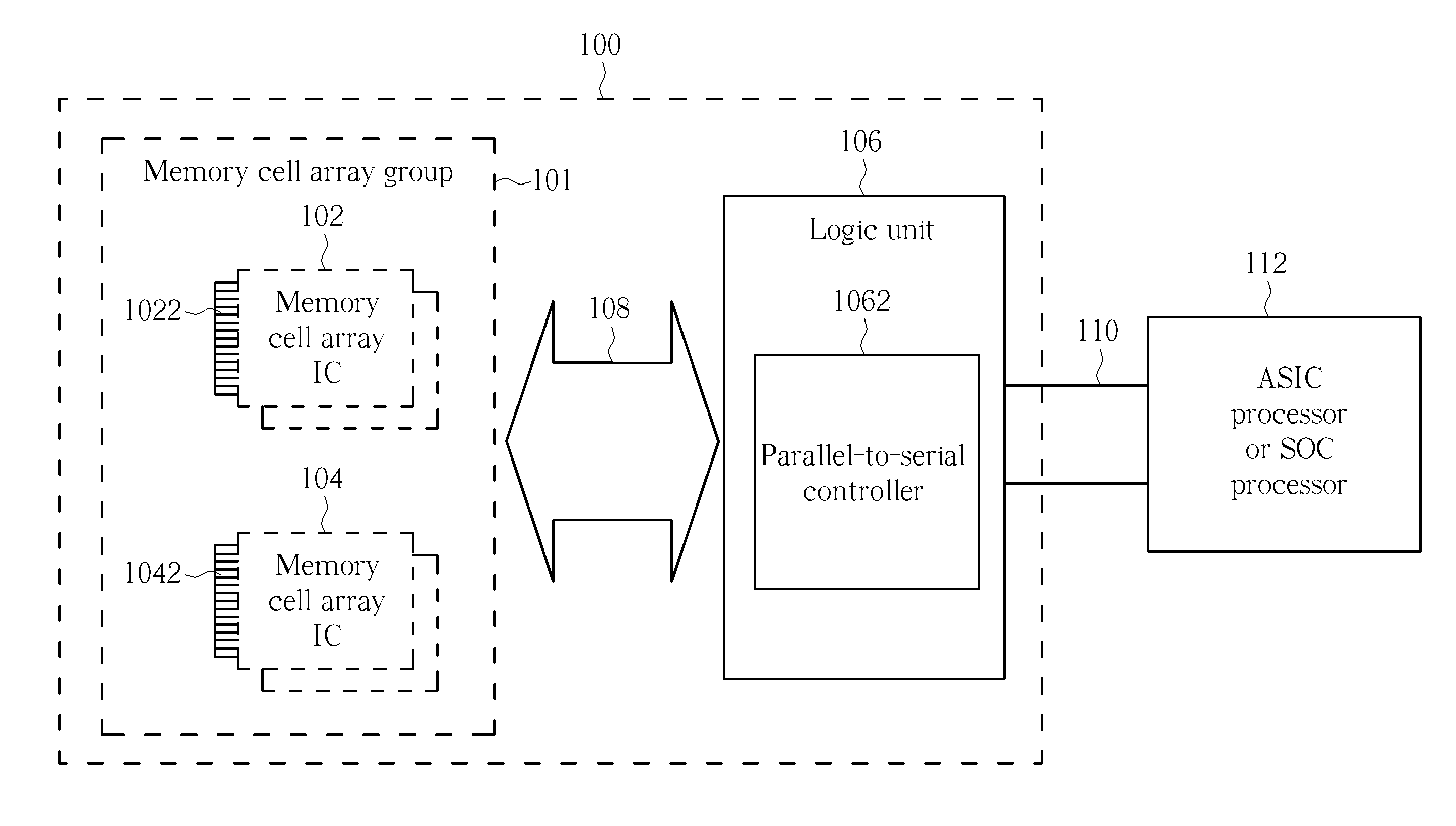
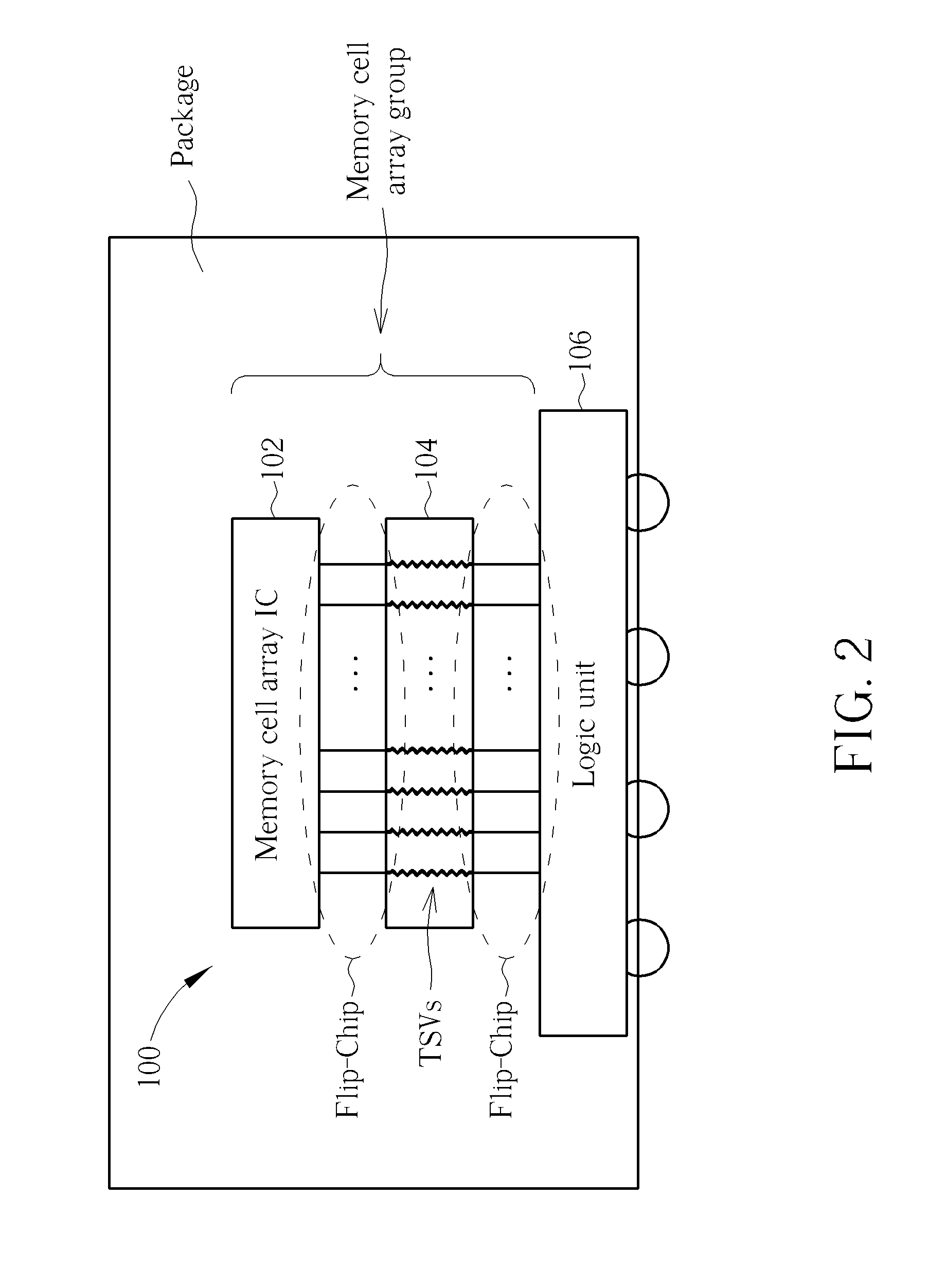
[0024]Please refer to FIG. 1. FIG. 1 is a diagram illustrating a high speed memory chip module 100 according to an embodiment. The high speed memory chip module 100 includes a type of memory cell array group 101 and a logic unit 106, where the type of memory cell array group 101 includes a memory cell array integrated circuit (IC) 102 which is a Dynamic Random Access Memory (DRAM) IC and a memory cell array IC 104 which is a flash or non-volatile memory (NVM) IC. But, the present invention is not limited to the high speed memory chip module 100 including the type memory cell array group 101 which includes the memory cell array IC 102 and the memory cell array IC 104, and also not limited to the memory cell array IC 102 being a DRAM IC and the memory cell array IC 104 being a flash or non-volatile memory IC. That is to say, the memory cell array IC 102 and the memory cell array IC 104 can also be other type of memory ICs. In addition, each of the memory cell array ICs 102, 104 has an...


PUM


Abstract

A high speed memory chip module includes a type of memory cell array group and a logic unit. The type memory cell array group includes multiple memory cell array integrated circuits (ICs), and each of the memory cell array ICs has a data bus and at least one memory cell array, and corresponds to first metal-oxide-semiconductor field-effect transistor (MOSFET) gate length corresponding to a first MOSFET process. The logic unit accesses the type of memory cell array group through a first transmission bus, where bus width of the first transmission bus is wider than bus width of the data bus of each of the memory cell array ICs. Corresponding to a second MOSFET process, the logic unit has a second MOSFET gate length which is shorter than the first MOSFET gate length.

Description

CROSS REFERENCE TO RELATED APPLICATIONS[0001]This application claims the benefit of U.S. Provisional Application No. 61 / 546,039, filed on Oct. 11, 2011 and entitled “High Speed Memory Platform,” the contents of which are incorporated herein by reference.BACKGROUND OF THE INVENTION[0002]1. Field of the Invention[0003]The present invention relates to a high speed memory chip module and a electronics system device with a high speed memory chip module, and particularly to a high speed memory chip module and an electronics system device with a high speed memory chip module that have lower power consumption, lower effective greenhouse gas emission rate, higher data transmission efficiency, enhanced electromagnetic interference (EMI) shielding effect, better heat dissipation capability, and an external noise isolation function.[0004]2. Description of the Prior Art[0005]Generally speaking, memories are usually designed as standard memory module or chip which are independent from logic units...

Claims


Application Information

Patent Timeline
IPC IPC(8): G11C7/10G06F13/40
CPCH01L2224/32225H01L2224/73265H01L2924/3025H01L2225/06568H01L2225/06541H01L2225/06513H01L2924/15311H01L2924/1434H01L2924/1431H01L2225/0651H01L2224/48227H01L2224/16225H01L2924/13091G06F13/40G11C7/10H01L2224/16145H01L2924/00012H01L2924/00G06F13/4018H01L24/73Y02D10/00
Inventor KEN, WENG-DAHLU, NICKY
Owner ETRON TECH INC
Why Eureka
Try Eureka