High Productivity Combinatorial Dual Shadow Mask Design

a dual-layer, high-efficiency technology, applied in the direction of vacuum evaporation coating, test/measurement of semiconductor/solid-state devices, coatings, etc., can solve the problem that the electrode size cannot be too small, and achieve the effect of small effective area, small area size, and simple and cost-effective device fabrication process

Active Publication Date: 2013-04-18
INTERMOLECULAR
View PDF11 Cites 19 Cited by
  • Summary
  • Abstract
  • Description
  • Claims
  • Application Information

AI Technical Summary

Benefits of technology

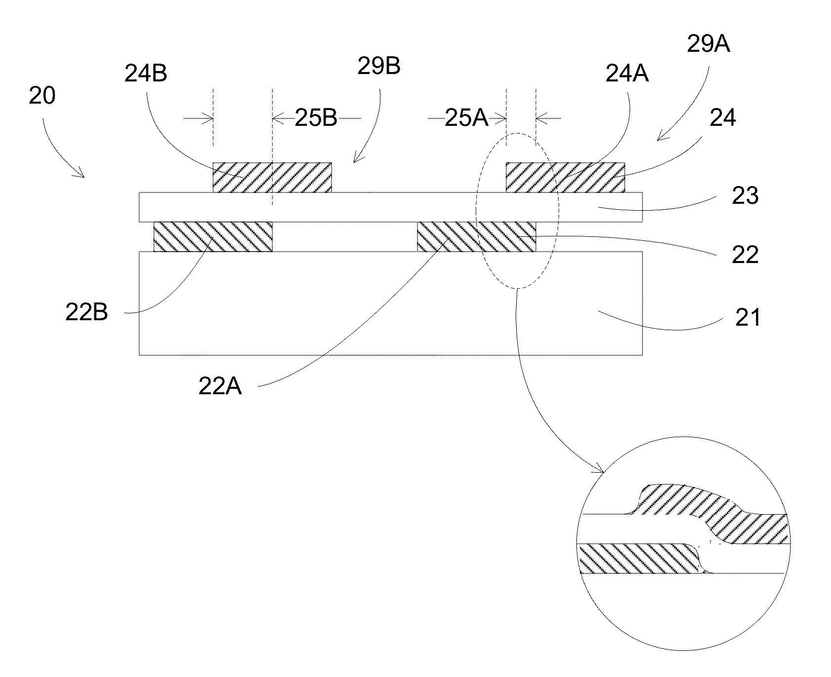
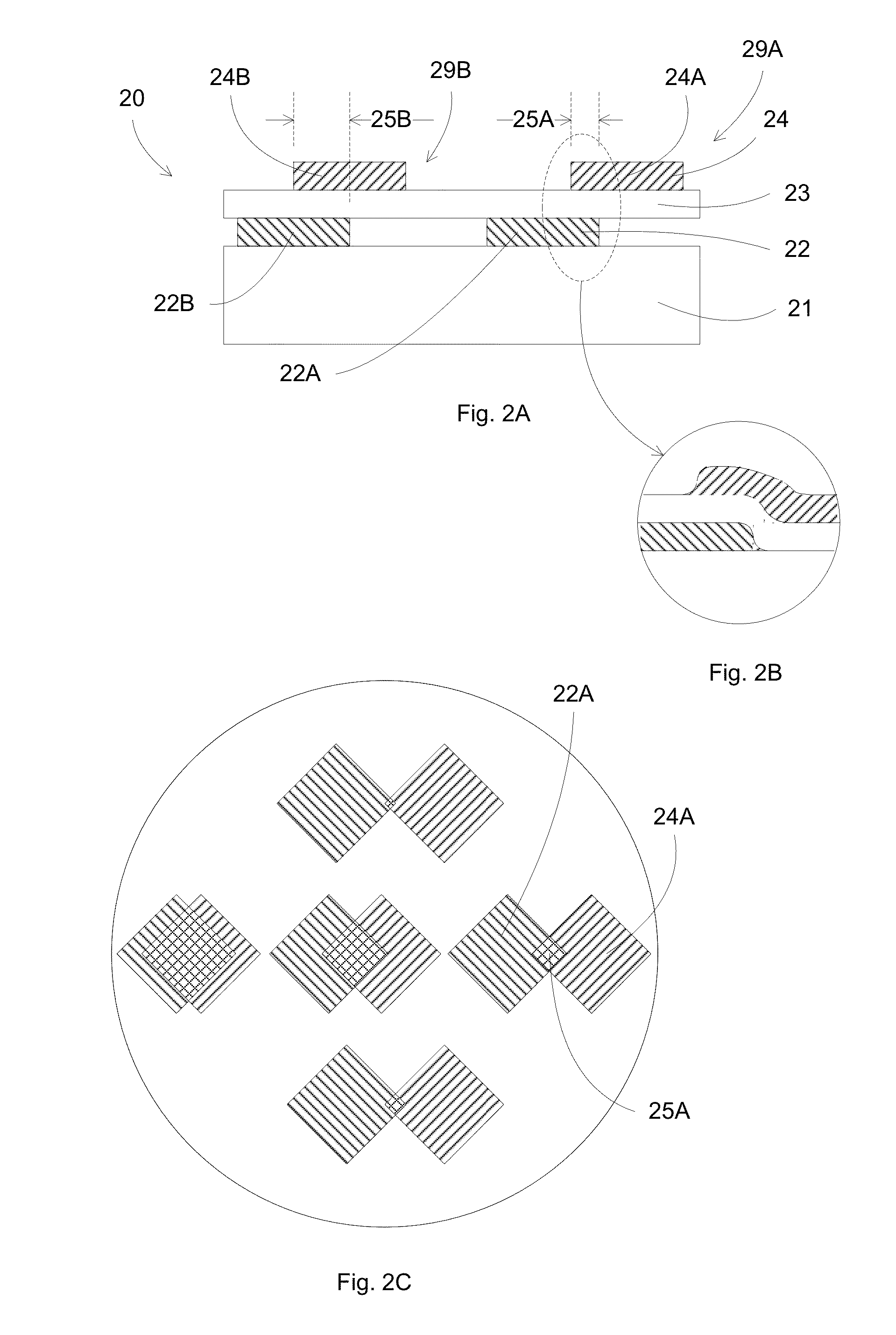
[0007]In some embodiments, the present invention discloses a dual shadow mask design to achieve capacitor structures with small effective areas. The capacitor structures can comprise a bottom and a top electrode patterned layers sandwiching a dielectric layer. The effective areas of the capacitors are the overlapping areas of ...

Problems solved by technology

However, a major limitation of shadow mask process is the electrode si...

Method used


Image

  • High Productivity Combinatorial Dual Shadow Mask Design
  • High Productivity Combinatorial Dual Shadow Mask Design
  • High Productivity Combinatorial Dual Shadow Mask Design

Examples


Embodiment Construction

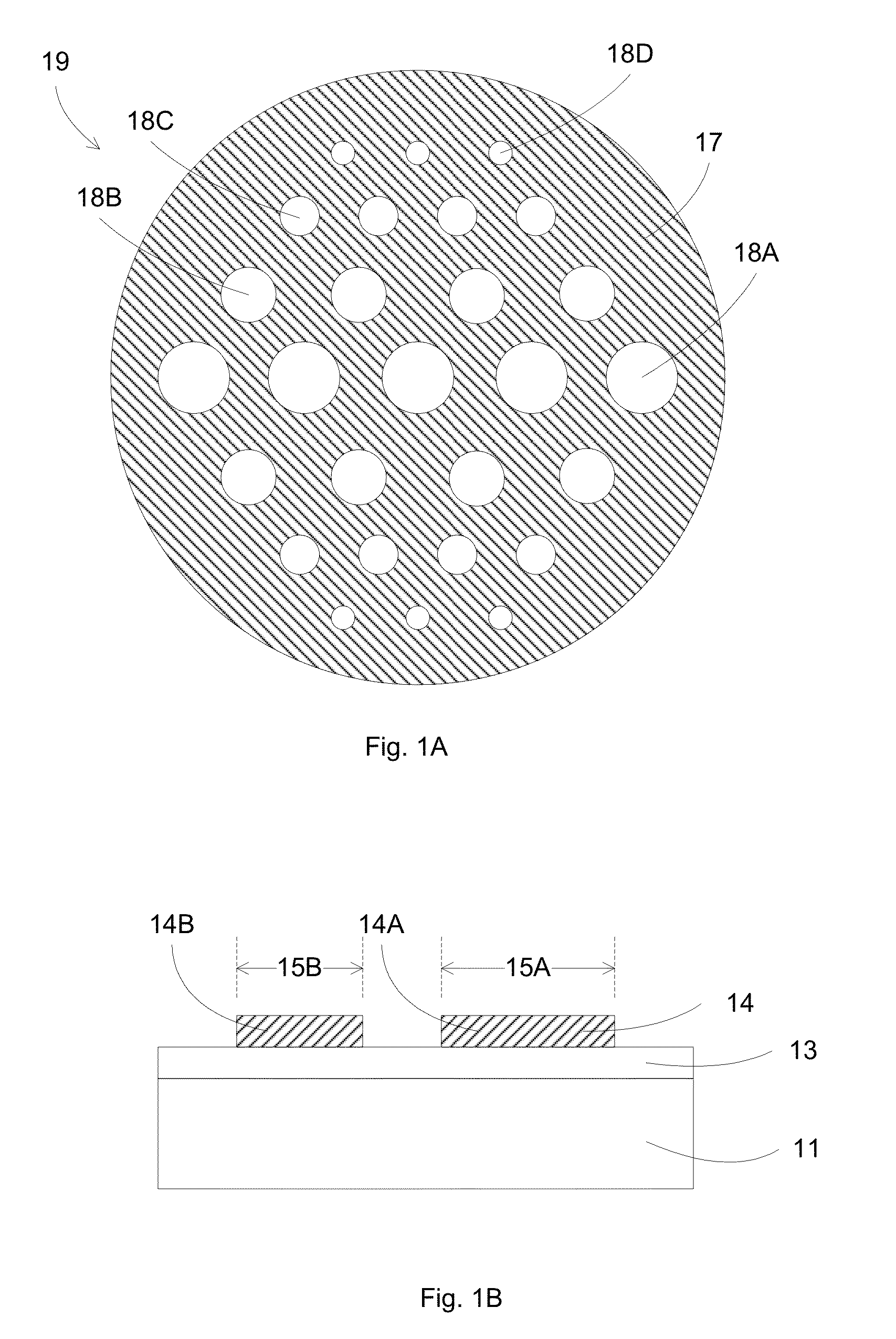
[0036]A detailed description of one or more embodiments is provided below along with accompanying figures. The detailed description is provided in connection with such embodiments, but is not limited to any particular example. The scope is limited only by the claims and numerous alternatives, modifications, and equivalents are encompassed. Numerous specific details are set forth in the following description in order to provide a thorough understanding. These details are provided for the purpose of example and the described techniques may be practiced according to the claims without some or all of these specific details. For the purpose of clarity, technical material that is known in the technical fields related to the embodiments has not been described in detail to avoid unnecessarily obscuring the description.

[0037]The present invention relates to dielectric testing, for example, to obtain optimum process and material conditions to achieve a desired performance. The tests can compr...


PUM

PropertyMeasurementUnit
Lengthaaaaaaaaaa
Thicknessaaaaaaaaaa
Sizeaaaaaaaaaa

Abstract

Dual shadow mask design can overcome the size and resolution limitations of shadow masks to provide capacitor structures with small effective areas. The capacitor structures have bottom and top electrode layers patterned using shadow masks, sandwiching a dielectric layer. The effective areas of the capacitors are the overlapping areas of the top and bottom electrodes, thus allowing small area sizes without subjected to the size limitation of the electrodes. The dual shadow mask design can be used in conjunction with high productivity combinatorial processes for screening and optimizing dielectric materials and fabrication processes.

Description

FIELD OF THE INVENTION[0001]The present invention relates generally to dielectric testing and particularly to capacitor structures fabricated using shadow mask designs.BACKGROUND OF THE INVENTION[0002]Deposition processes are commonly used in semiconductor manufacturing to deposit a layer of material onto a substrate. Processing is also used to remove layers, defining features (e.g., etch), preparing layers (e.g., cleans), doping or other processes that do not require the formation of a layer on the substrate. Processes and process shall be used throughout the application to refer to these and other possible known processes used for semiconductor manufacturing and any reference to a specific process should be read in the context of these other possible processes. In addition, similar processing techniques may apply to the manufacture of integrated circuits (IC) semiconductor devices, flat panel displays, optoelectronics devices, data storage devices, magneto electronic devices, magn...

Claims


Application Information

Patent Timeline
IPC IPC(8): H01L29/92H01L21/02
CPCC23C14/042H01L29/94H01L27/3295H01L22/34H01L28/60B01J19/0046B01J2219/0043B01J2219/0075
Inventor ANANTHAN, VENKATPHATAK, PRASHANT B.
Owner INTERMOLECULAR
Why Eureka
Try Eureka