

Digital phase locked loop
a digital phase and lock loop technology, applied in the field of electronic devices, can solve the problems of difficult implementation of traditional analog circuits, difficult to integrate analog basebands with digital basebands, and inability to solve the problem of reducing the effect of communication, and eliminating unnecessary circuitry
- Summary
- Abstract
- Description
- Claims
- Application Information
AI Technical Summary
Benefits of technology
Problems solved by technology
Method used
Image

Examples
first embodiment
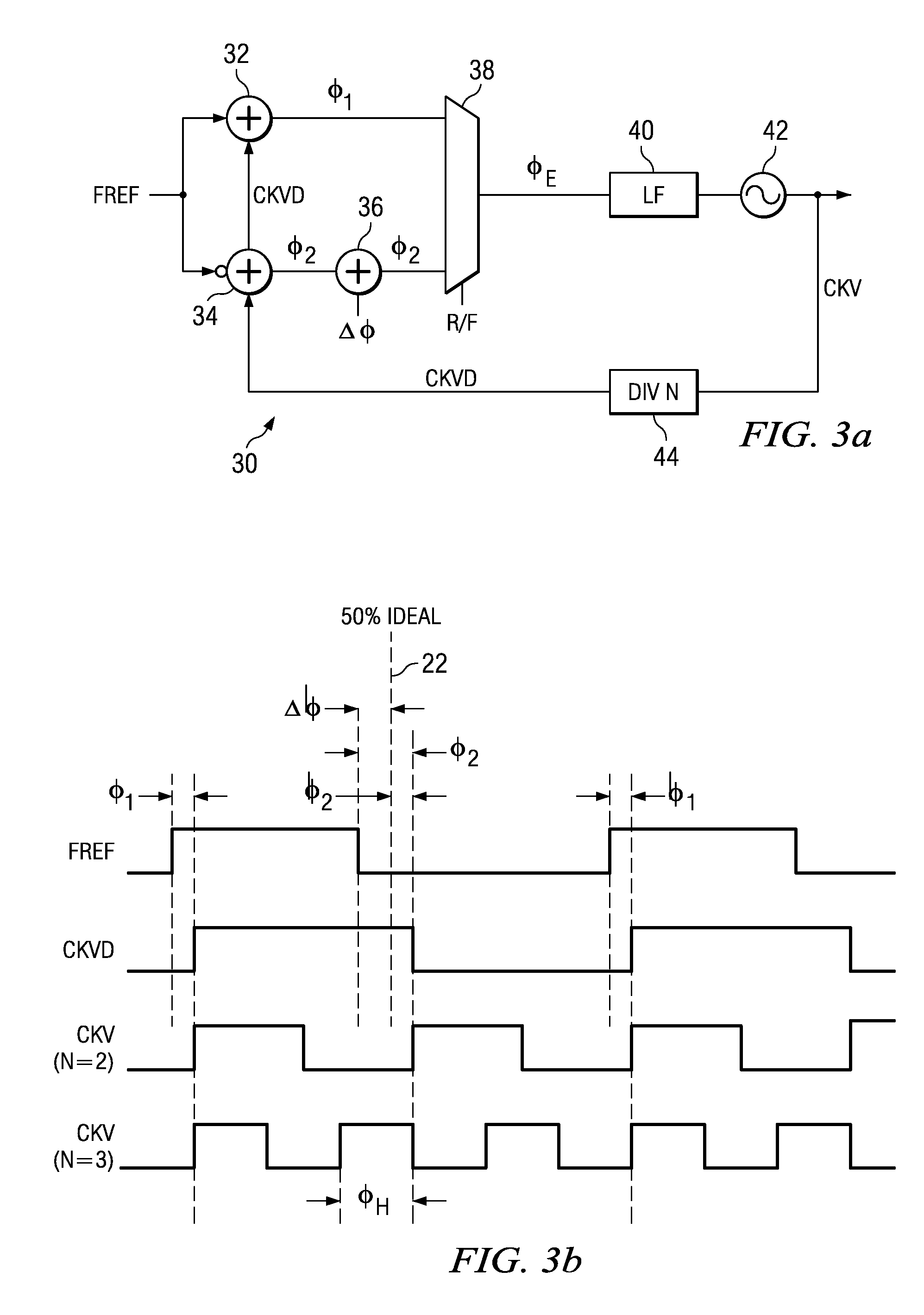
[0040]FIG. 3a illustrates the invention for using both edges of a reference clock in a PLL 30. FREF is input to a first phase detector 32 (which compares phase information on a first active edge, e.g. rising edge) of FREF and a second phase detector 34 (which compares phase information on a second active edge, e.g. falling edge) of FREF. Alternatively, the FREF signal is input to the first phase detector 32 and the inverted FREF signal is input to the second phase detector 34, and both phase detectors operate internally on the same active edge of the reference clock signals that are 180 degrees out of phase. The output of the first phase detector 32 is a first error signal φ1 and the output of the second phase detector 34 is a second intermediate error signal φ2′. The intermediate error signal φ2′ is added to Δφ through phase offset adder 36 to generate the second error signal φ2. The first and second error signals are input to multiplexer 38, which selects one of the first and seco...
second embodiment
[0042]It would also be possible to compare the edges of FREF with the output CKV. In this case, both the rising edge and falling edge of FREF would be compared to a rising edge of CKV, if N (fCKV / fFREF) was an even integer. If N is an odd integer, two approaches could be used. In the first approach, rising edges of FREF would be compared to rising edges of CKV and falling edges of FREF would be compared to falling edges of CKV (it would also be possible to compare rising edges of FREF to falling edges of CKV and vice-versa). In the second embodiment, a half-phase adjustment φH could be added to φ2′ along with Δφ by the phase offset adder 36, such that φ2=φ2′+Δφ+φH.
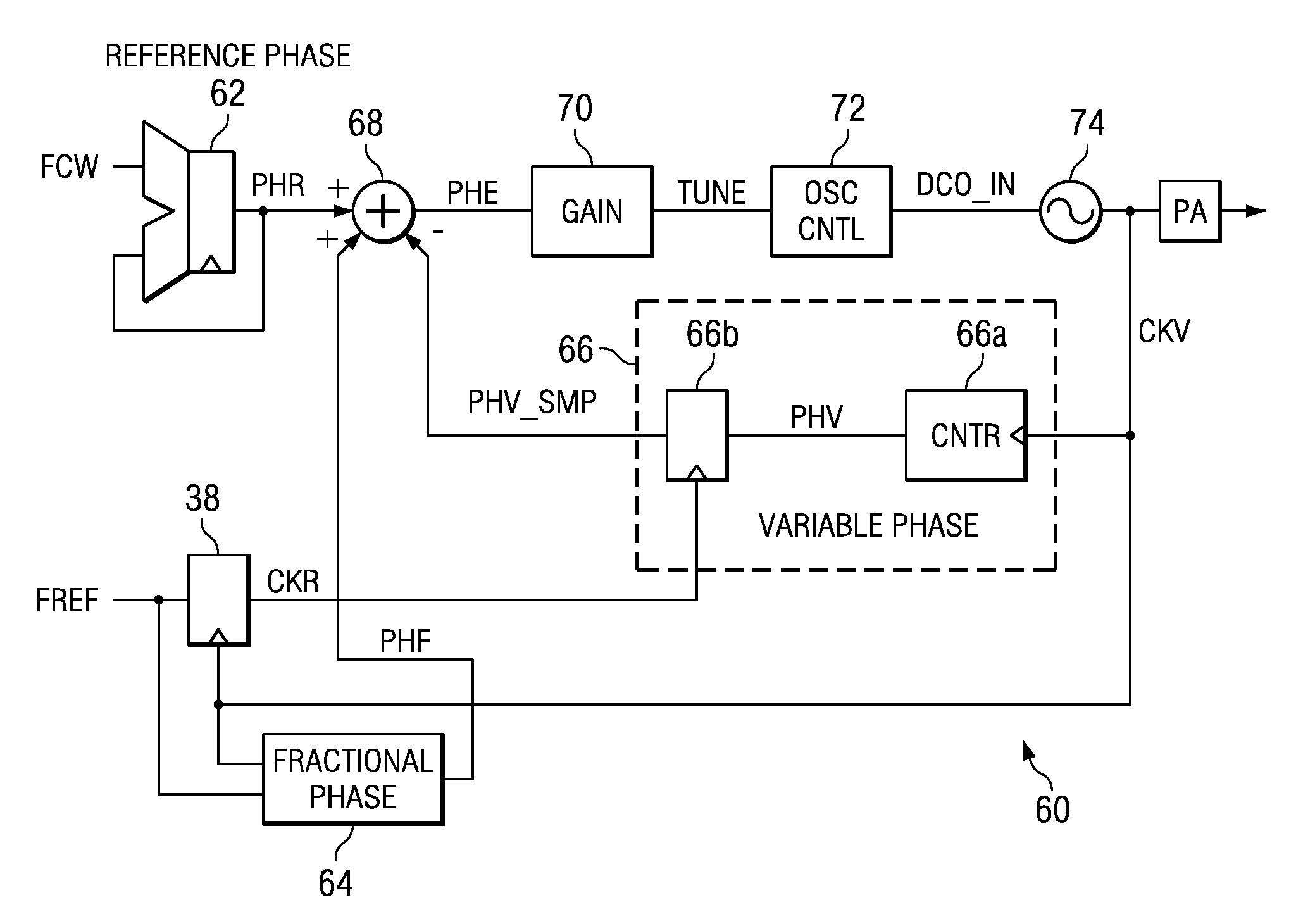
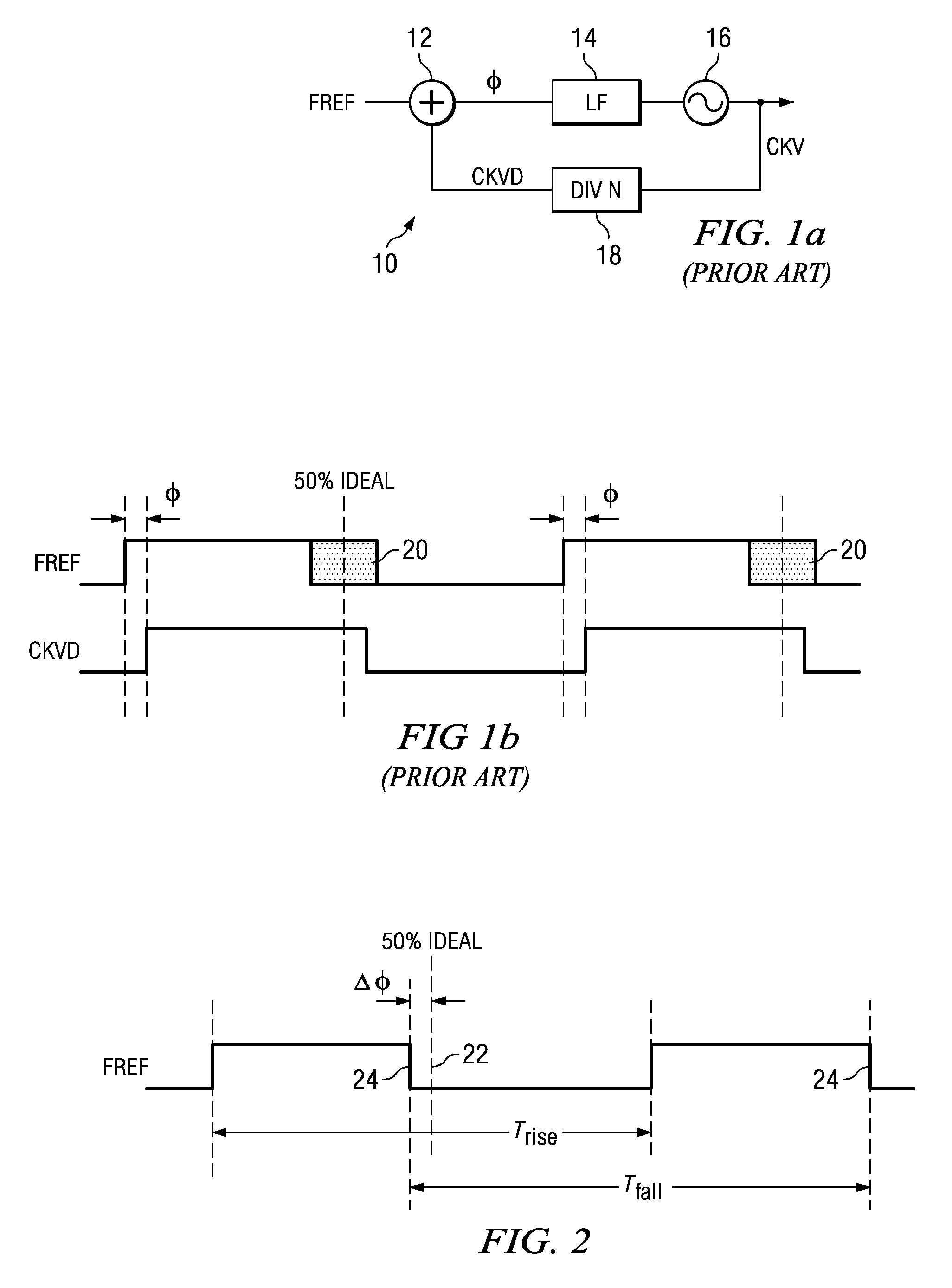
[0043]FIG. 4a illustrates a block diagram of an all digital PLL (ADPLL) 60 of the type disclosed in U.S. Ser. No. 10 / 008,462 to Staszewski et al, entitled “Frequency Synthesizer with Phase Restart”, filed Nov. 30, 2001, which is incorporated by reference herein. This ADPLL is designed to work off a single edge of FREF.
[004...
PUM
 Abstract
Description
Claims
Application Information