Mask ROM fabrication method

a mask rom and fabrication method technology, applied in the field of mask rom technology, can solve the problem of hard to reduce the overall area and achieve the effect of hard to further reduce the size of the mask rom

Active Publication Date: 2013-04-18
NYQUEST +1
View PDF0 Cites 2 Cited by
  • Summary
  • Abstract
  • Description
  • Claims
  • Application Information

AI Technical Summary

Benefits of technology

[0005]The primary objective of the present invention is to over...

Problems solved by technology

Thus, it is hard for mask ROM to reduce the overall area, i...

Method used


Image

  • Mask ROM fabrication method
  • Mask ROM fabrication method
  • Mask ROM fabrication method

Examples


Embodiment Construction

[0033]The embodiments are used to describe the technical contents of the present invention in detail in cooperation with the drawings below.

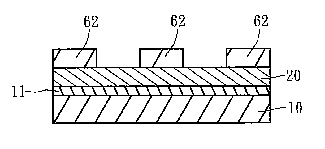
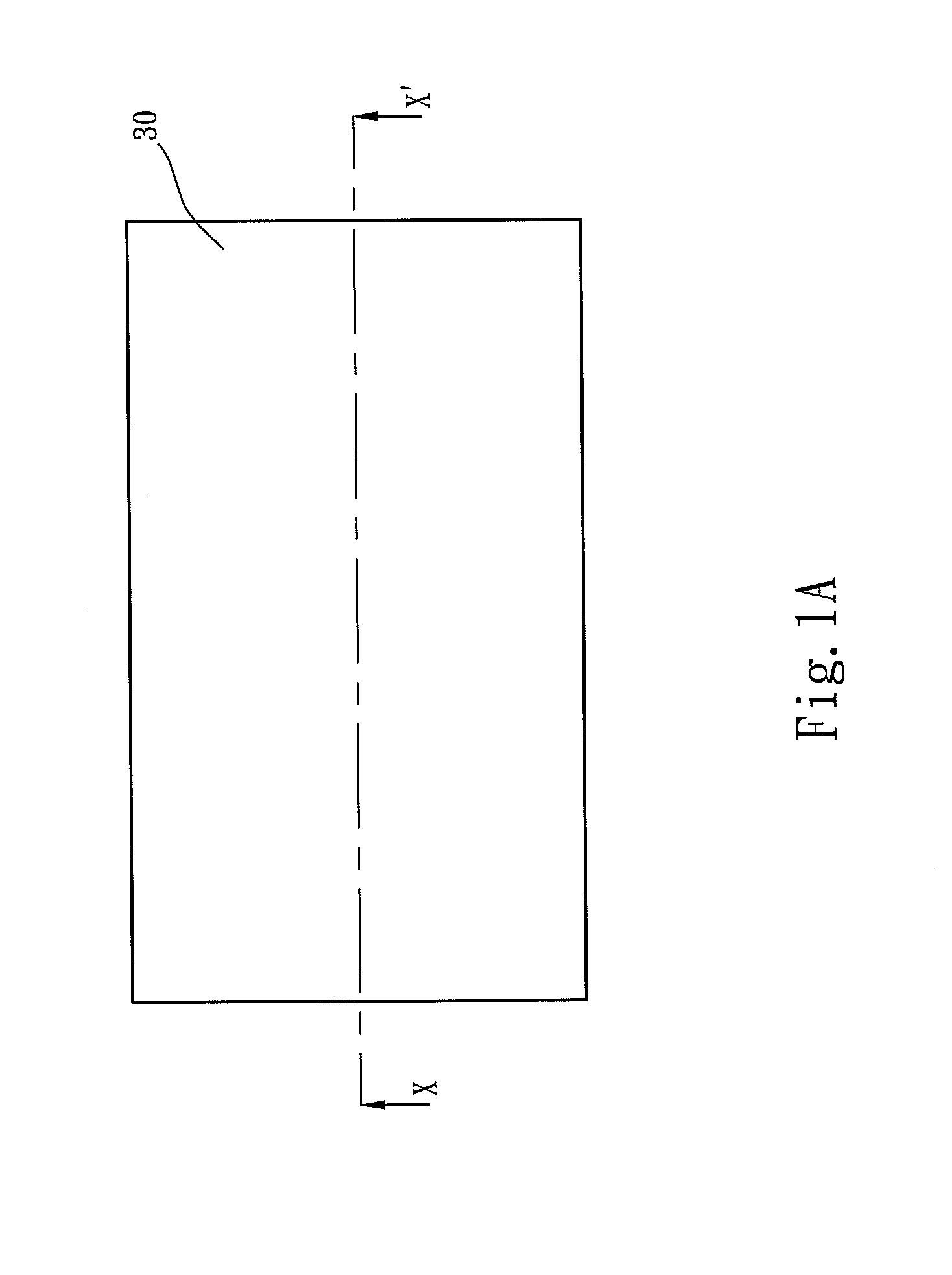
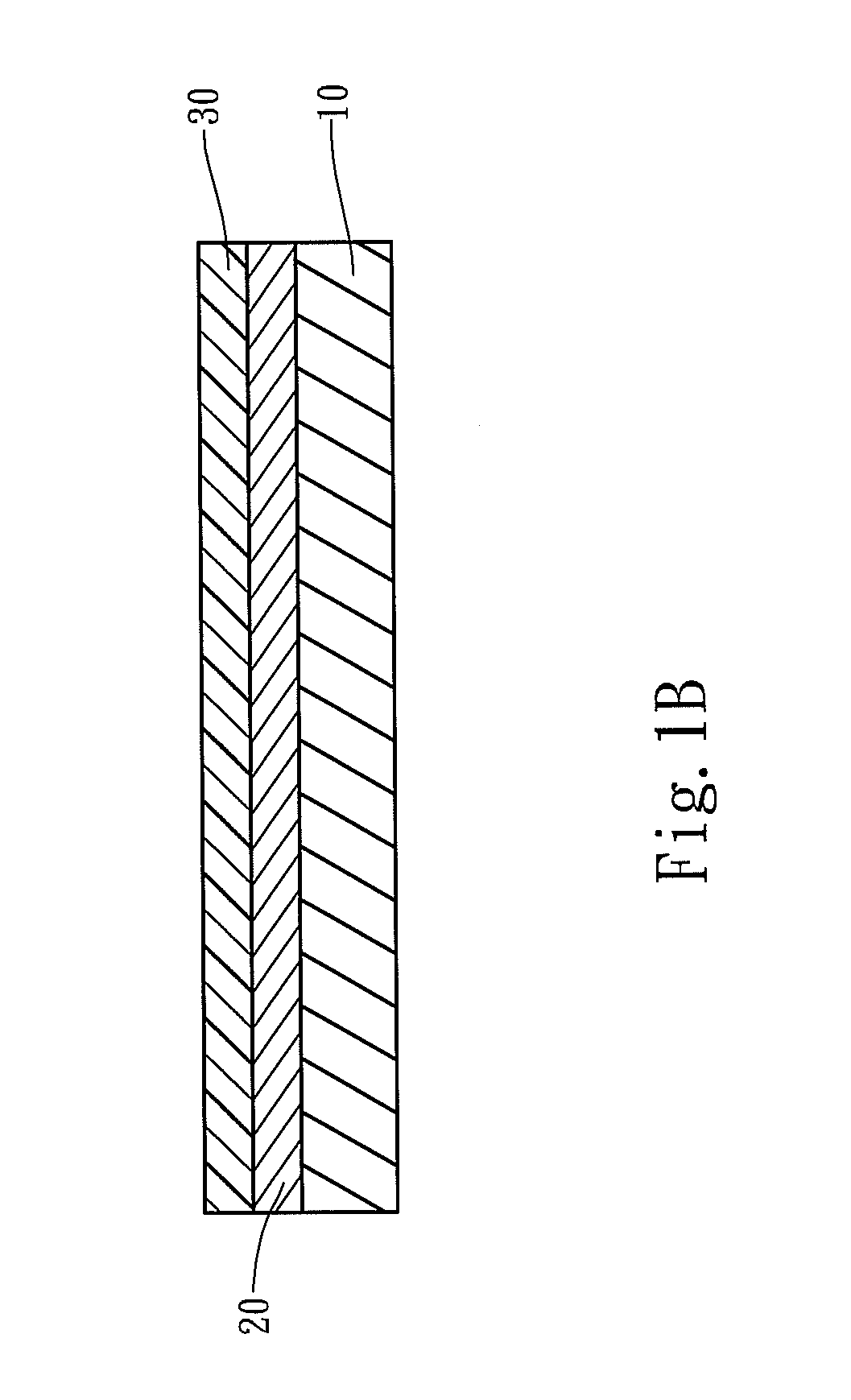
[0034]Refer to FIG. 1A and FIG. 1B. The mask ROM fabrication method of the present invention comprises the following steps.

[0035]In Step 1, form a gate dielectric layer 20 on a substrate 10 and a first photoresist layer 30 on the gate dielectric layer 20. In one embodiment, the substrate 10 is a silicon substrate doped with a p-type dopant, wherein the p-type dopant is selected from a group consisting of boron, indium, aluminum, and gallium. Silicon dioxide is grown on the substrate 10 to form the gate dielectric layer 20. Next, photoresist is spin-coated on the gate dielectric layer 20 to form the first photoresist layer 30. In this embodiment, the first photoresist layer 30 is exemplified by a positive photoresist layer. However, a negative photoresist may also be used as the material of the first photoresist layer 30 in the present invention....


PUM


Abstract

A mask ROM fabrication method which comprises steps: sequentially forming a gate dielectric layer and a first photoresist layer on a substrate; letting a light having a wavelength of 365 nm pass through a first phase shift mask to photolithographically form on the first photoresist layer a plurality of first trenches having a width of 243-365 nm; doping the substrate to form a plurality of embedded bit lines having a width of 243-365 nm; removing the first photoresist layer; sequentially forming a polysilicon layer and a second photoresist layer on the gate dielectric layer; and letting the light pass through a second phase shift mask to photolithographically form a plurality of polysilicon word lines on the polysilicon layer. Thereby is reduced the line width of mask ROM to 243-365 nm and decreased the area of mask ROM.

Description

FIELD OF THE INVENTION[0001]The present invention relates to a mask ROM technology, particularly to a mask ROM fabrication method.BACKGROUND OF THE INVENTION[0002]Memories may be categorized into ROM (Read Only Memory) and RAM (Random Access Memory). ROM can keep data without electricity. RAM loses data stored thereinside once power is turned off. ROM can be further classified into mask ROM, EPROM (Erasable Programmable ROM), EEPROM (Electrically Erasable Programmable ROM), and flash memory. As disclosed in a U.S. Pat. No. 5,514,610, high-energy ion is used to write data in mask ROM. Once data has been written into mask ROM, the user cannot erase or rewrite the data but can only read the data. Therefore, mask ROM normally applies to the products that data is not intended to vary in the future, such as the booting programs for computers / embedded devices, font tables, and programs for game machines. Mask ROM has the advantage of the lowest cost per bit.[0003]Mask ROM normally adopts c...

Claims


Application Information

Patent Timeline
IPC IPC(8): H01L21/336
CPCH01L21/0274H01L27/11253H01L21/32139H10B20/38
Inventor CHEN, KUANG-CHUCHEN, CHENG TAOHSU, CHUNG-LUNGCHIU, CHUN-YAOCHANG, CHIN-YUNG
Owner NYQUEST
Why Eureka
Try Eureka