Semiconductor device and method for manufacturing the same

a semiconductor memory device and semiconductor technology, applied in the direction of semiconductor memory devices, electrical devices, transistors, etc., can solve the problems of reducing the reliability of the device, increasing the capacitance, and reducing the refresh characteristic of the semiconductor memory device, so as to reduce the size of the pattern, improve the operating characteristic of the device, and remove the gap-filling defect of the gate material

Inactive Publication Date: 2013-04-25
SK HYNIX INC
View PDF9 Cites 7 Cited by
  • Summary
  • Abstract
  • Description
  • Claims
  • Application Information

AI Technical Summary

Benefits of technology

[0016]Various embodiments of the invention are directed to forming a space where a buried gate is to be formed in a dummy region of a mat edge larger than in the conventional art, thereby preventing

Problems solved by technology

Thereby, short channel effect and drain induced barrier lowering (DIBL) in a conventional transistor are caused, and thus reliability is degraded.
However, with reduction of the design rule to below 100 nm, increase of the doping concentration in the channel region causes an electric field in a storage node junction to increase, thereby resulting in degradation of refresh characteristic in semiconductor memory devices.
Thereby, parasitic capacitance is increased and an operation margin of a sense amplifier amplifying data transferred through the bit line is degraded, which has a negative effect on the reliability of a semiconductor device.
However, in the process for forming th

Method used


Image

  • Semiconductor device and method for manufacturing the same
  • Semiconductor device and method for manufacturing the same
  • Semiconductor device and method for manufacturing the same

Examples


Embodiment Construction

[0058]Exemplary embodiments of the present invention will be described in detail with reference to the attached drawings.

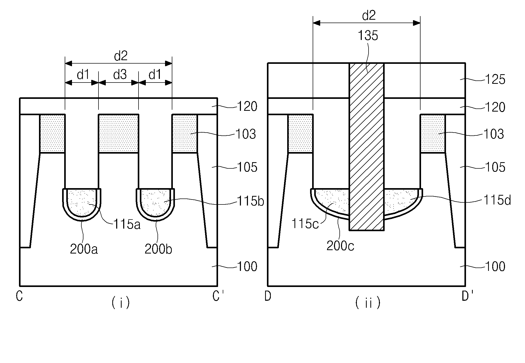
[0059]Referring to FIGS. 3A-3B and 4E, an embodiment according to the present invention includes a first active region (A1) formed in a cell region of a substrate (100) and a second active region (A2) formed in a dummy region of the substrate. The dummy region extends from the cell region. In FIG. 4E, (i) denotes a cell region and (ii) denotes a dummy region.

[0060]First and second buried cell gate (115a, 115b) are arranged in parallel to each other and pass across the first active region (A1). First and second buried dummy gate (115c, 115d) are arranged in parallel to each other and pass across the first active region (A2).

[0061]A conductive pattern is formed between the first and second buried cell gates (115a, 115b). An insulating film (135) is formed between the first and second buried dummy gates (115c, 115d). The first and the second buried cell gates (115a, ...


PUM


Abstract

A semiconductor device comprises a buried gate formed in a mat and in an adjacent dummy region. A space larger than is conventional is formed in a dummy region of a mat edge where the buried gate is to be created. This larger space inhibits shortening of an end of a buried gate and reduction in pattern size attributable to lithographic distortion arising between patterned (mat) and unpatterned (dummy) regions. Device reliability is thereby improved by avoiding gap-fill defects of a gate material.

Description

CROSS-REFERENCE TO RELATED APPLICATION[0001]The present application claims priority to Korean patent application No. 10-2011-0108823 filed on Oct. 24, 2011, which is incorporated by reference in its entirety.BACKGROUND OF THE INVENTION[0002]1. Technical Field[0003]The inventive concept relates generally to a semiconductor device and a method for manufacturing the same, and more particularly to a semiconductor device comprising a buried gate disposed in a dummy region of an edge of a cell region and a method for manufacturing the same.[0004]2. Related Art[0005]Semiconductor devices include a plurality of unit cells including a capacitor and a transistor. The capacitor is used to store data and the transistor is used to transfer data between the capacitor and a bit line in response to a control signal (a word line) using a semiconductor property in which electric conductivity is changed according to conditions. The transistor has three parts: a gate, a source, and a drain. Charges mov...

Claims


Application Information

Patent Timeline
IPC IPC(8): H01L27/108H01L21/28H01L29/78
CPCH01L29/42356H01L27/10894H01L27/10891H01L27/10876H10B12/053H10B12/488H10B12/09H01L21/76831H01L29/4236H01L29/66045H01L29/66712
Inventor KIM, SE HYUN
Owner SK HYNIX INC
Why Eureka
Try Eureka