Solar wafer electrostatic chuck

a solar cell and electrostatic technology, applied in the field of solar cell processing, can solve the problems of high utilization rate, no cooling fluid connection, and high cost of purchasing and operating a solar cell processing system, and achieve the effect of high throughput processing

Inactive Publication Date: 2013-05-02
INTEVAC
View PDF10 Cites 12 Cited by
  • Summary
  • Abstract
  • Description
  • Claims
  • Application Information

AI Technical Summary

Benefits of technology

[0011]Various embodiments provide an electrostatic chuck which is designed to endure high throughput processing, such as that used in solar fabrication systems, and can wi

Problems solved by technology

On the other hand, the cost of purchasing and operating a solar cell processing system must be very low.
However, the electrostatic chuck for solar cell system must cost a fraction of that for an IC manufacturing, yet it must e

Method used


Image

  • Solar wafer electrostatic chuck
  • Solar wafer electrostatic chuck
  • Solar wafer electrostatic chuck

Examples


Embodiment Construction

[0021]Various features of the electrostatic chuck according to embodiments of the invention will now be described with reference to the drawings. The description will include examples of electrostatic chuck, processing systems incorporating the electrostatic chuck, and methods for making the electrostatic chuck for fabrication of, e.g., solar cells.

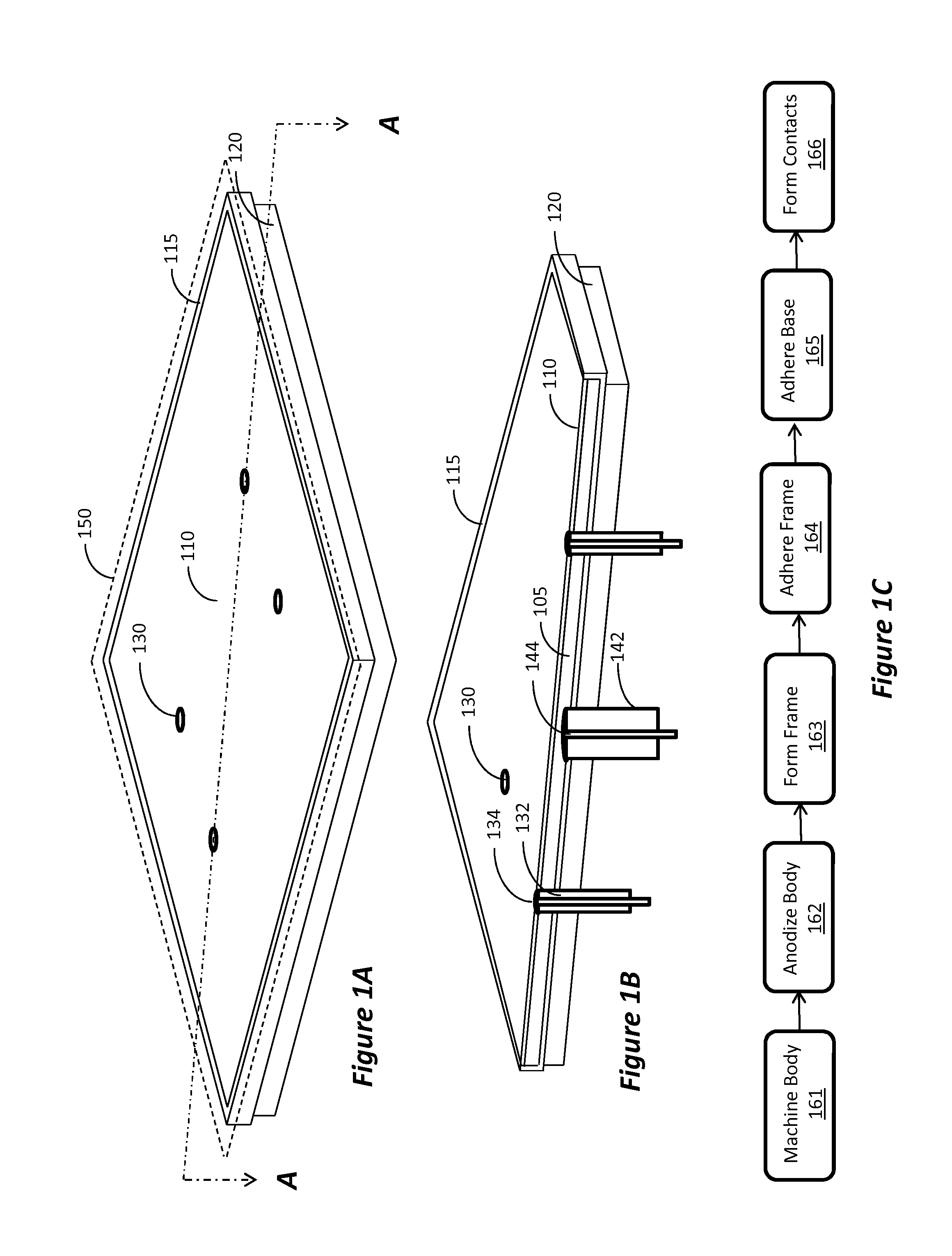
[0022]FIG. 1A is a schematic illustrating the major parts of an electrostatic chuck according to one embodiment, while FIG. 1B illustrates a partial cross-section along line A-A of FIG. 1A. The chucks body 105 is made of aluminum slab and is configured to have sufficient thermal mass to control heating of the chuck during plasma processing. The top surface of the body 105 is anodized, thereby forming electrically insulating anodized aluminum layer 110. The sides of the chuck are encased by ceramic layer or frame 115. Ceramic layer 115 may be a ceramic coating applied to all four sides of the aluminum body, e.g, using standard plasma spray...


PUM

PropertyMeasurementUnit
Thicknessaaaaaaaaaa
Electric potential / voltageaaaaaaaaaa

Abstract

An electrostatic chuck is disclosed, which is especially suitable for fabrication of substrates at high throughput. The disclosed chuck may be used for fabricating large substrates or several smaller substrates simultaneously. For example, disclosed embodiments can be used for fabrication of multiple solar cells simultaneously, providing high throughput. An electrostatic chuck body is constructed using aluminum body having sufficient thermal mass to control temperature rise of the chuck, and anodizing the top surface of the body. A ceramic frame is provided around the chuck's body to protect it from plasma corrosion. If needed, conductive contacts are provided to apply voltage bias to the wafer. The contacts are exposed through the anodization.

Description

RELATED APPLICATION[0001]This application claims priority benefit from U.S. Provisional Application Ser. No. 61 / 554,457, filed on Nov. 1, 2011, the content of which is incorporated herein by reference in its entirety.BACKGROUND[0002]1. Field[0003]This disclosure relates to processing of solar cells and, in particular, to electrostatic chucks supporting wafers inside solar cells processing chambers.[0004]2. Related Art[0005]Processing chambers, such as plasma chambers, used to fabricate solar cells have the same basic elements of processing chambers used for fabricating integrated circuits (IC), but have different engineering and economic requirements. For example, while chambers used to fabricate integrated circuits have throughput on the order of a few tens of wafers per hour, chambers used for fabricating solar are required to have throughput on the order of a few thousands of wafers per hour. On the other hand, the cost of purchasing and operating a solar cell processing system m...

Claims


Application Information

Patent Timeline
IPC IPC(8): H02N13/00H01L31/18
CPCH02N13/00H01L31/18Y10T29/49117H01J2237/16H01L21/6833
Inventor CHO, YOUNG KYUJANAKIRAMAN, KARTHIKBLUCK, TERRYKEDLAYA, DIWAKAR
Owner INTEVAC
Why Eureka
Try Eureka