Organic light-emitting device

a light-emitting device and organic technology, applied in the direction of thermoelectric device junction materials, semiconductor devices, electrical apparatus, etc., can solve the problems of large reflection loss of light accompanying the propagation of light in the device, the propagate behind the substrate to directly become a loss, and the difficulty in efficiently extracting light trapped in the substrate, etc., to achieve high work function, low ionization potential, and high hole mobility

Inactive Publication Date: 2013-05-09
HITACHI LTD
View PDF0 Cites 6 Cited by
  • Summary
  • Abstract
  • Description
  • Claims
  • Application Information

AI Technical Summary

Benefits of technology

[0020]The transparent electrode 2 formed as an anode is an electrode for injecting holes into the organic light-emitting layer 3. As the transparent electrode 2 (anode), an electrode material composed of a metal, an alloy, an electroconductive compound, or a mixture thereof, each having a high work function is preferably used, and particularly, an electrode material having a work function of 4 eV or more is preferably used. Specific examples of such an electrode material include metals such as gold and conductive transparent materials such as CuI, ITO (indium tin oxide), SnO2, ZnO, and IZO (indium zinc oxide). For example, by depositing such an electrode material on the front substrate 1 using a vacuum deposition method, a sputtering method, a CVD method, an ion plating method, a coating method, or the like, the transparent electrode 2 (anode) in the form of a thin film can be formed. The light transmittance of the transparent electrode 2 (anode) is preferably 80% or more. Further, the sheet resistance of the transparent electrode 2 (anode) is preferably several hundreds Ω / sq. or less, particularly preferably 100 Ω / sq. or less. Further, in order to control the properties of the transparent electrode 2 (anode) such as transparency and conductivity as described above, the film thickness of the transparent electrode 2 (anode) is set to 80 to 400 nm, more preferably 100 to 200 nm, although it varies depending on the material thereof.
[0021]The organic light-emitting layer 3 is composed of a hole transport layer, a light-emitting layer, an electron transport layer, a buffer layer, and the like. However, the organic light-emitting layer may not have a hole transport layer, an electron transport layer, or a buffer layer as long as it has at least a light-emitting layer. Further, the organic light-emitting layer may have a hole injection layer or an electron injection layer, which will be described later, in some cases.
[0022]The hole transport layer has a function of transporting holes and injecting the holes into the light-emitting layer. Therefore, the hole transport layer is preferably composed of a hole transport material having a high hole mobility. Further, it is preferred that the hole transport layer is chemically stable and has a low ionization potential, a low electron affinity, and a high glass transition temperature. As a material of the hole transport layer, for example, N,N′-bis(3-methylphenyl)-N,N′-diphenyl-[1,1′-biphenyl]-4,4′-diamine (TPD), 4,4′-bis[N-(1-naphthyl)-N-phenylamino]biphenyl (α-NPD), 4,4′,4″-tri(N-carbazolyl)triphenylamine (TCTA), 1,3,5-tris[N-(4-diphenylaminophenyl)phenylamino]benzene (p-DPA-TDAB), 4,4′,4″-tris(N-carbazol)triphenylamine (TCTA), 1,3,5-tris[N,N-bis(2-methylphenyl)-amino]-benzene (o-MTDAB), 1,3,5-tris[N,N-bis(3-methylphenyl)-amino]-benzene (m-MTDAB), 1,3,5-tris[N,N-bis(4-methylphenyl)-amino]-benzene (p-MTDAB), 4,4′,4″-tris[1-naphthyl(phenyl)amino]triphenylamine (1-TNATA), 4,4′,4″-tris[2-naphthyl(phenyl)amino]triphenylamine (2-TNATA), 4,4′,4″-tris[biphenyl-4-yl-(3-methylphenyl)amino]triphenylamine (p-PMTDATA), 4,4′,4″-tris[9,9-dimethylfluorene-2-yl(phenyl)amino]triphenylamine (TFATA), 4,4′,4″-tris(N-carbazoyl)triphenylamine (TCTA), 1,3,5-tris[N-(4-diphenylaminophenyl)phenylamino]benzene (p-DPA-TDAB), 1,3,5-tris{4-[methylphenyl(phenyl)amino]phenyl}benzene (MTDAPB), N,N′-di(biphenyl-4-yl)-N,N′-diphenyl[1,1′-biphenyl]-4,4′-diamine (p-BPD), N,N′-bis(9,9-dimethylfluorene-2-yl)-N,N′-diphenylfluorene-2,7-diamine (PFFA), N,N,N′,N′-tetrakis(9,9-dimethylfluoren-2-yl)-[1,1-biphenyl]-4,4′-diamine (FFD), (NDA)PP, 4-4′-bis[N,N′-(3-tollyl)amino]-3-3′-dimethylbiphenyl (HMTPD), etc. are preferred, and these may be used alone or in combination of two or more of them.
[0023]A hole injection layer may be disposed between the transparent electrode 2 serving as an anode and the hole transport layer as needed. The hole injection layer is preferably formed from a material having an appropriate ionization potential so as to reduce a hole injection barrier between the anode and the hole transport layer. Further, it is preferred that the hole injection layer plays a role in burying the unevenness of a surface of an under layer. Examples of the material of the hole injection layer include copper phthalocyanine, a star burst amine compound, polyaniline, polythiophene, vanadium oxide, molybdenum oxide, ruthenium oxide, and aluminum oxide.
[0024]The hole transport material may contain an oxidant. By incorporating an oxidant in the hole transport material, the barrier between the anode and the hole transport layer can be reduced, or the electroconductivity can be improved. Examples of the oxidant include Lewis acid compounds such as ferric chloride, ammonium chloride, gallium chloride, indium chloride, and antimony pentachloride, electron accepting compounds such as trinitrofluorene, and compounds listed as the material of the hole injection layer such as vanadium oxide, molybdenum oxide, ruthenium oxide, and aluminum oxide, and these may be used alone or in combination of two or more of them.
[0025]As a luminescent organic compound to be used in the light-emitting layer, an arbitrary known compound can be used, and examples thereof include anthracene, naphthalene, pyrene, tetracene, coronene, perylene, phthaloperylene, naphthaloperylene, diphenylbutadiene, tetraphenylbutadiene, coumarin, oxadiazole, bisbenzoxazoline, bisstyryl, cyclopentadiene, quinoline metal complexes, tris(8-hydroxyquinolinate)aluminum complexes, tris(4-metal-8-quinolinate)aluminum complexes, tris(5-phenyl-8-quinolinate)aluminum complexes, aminoquinoline metal complexes, benzoquinoline metal complexes, tri-(p-terphenyl-4-yl)amine, 1-aryl-2,5-di(2-thienyl)pyrrole derivatives, pyran, quinacridone, rubrene, distyrylbenzene derivatives, distyrylarylene (DSA) derivatives, and compounds having such a luminescent organic compound in the molecule, however, it is not limited thereto. Further, not only compounds derived from fluorescent pigments typified by these compounds, but also materials capable of phosphorescence emission from a state of triplet and compounds having a group derived from such a material in a part of the molecule can also be preferably used.

Problems solved by technology

However, in the configuration described in Patent document 1, the reflector is formed only in a side surface and an inner portion of the substrate, and therefore, part of light reflected by the reflector exits ahead of the substrate to contribute to the improvement of the light extraction efficiency, however, on the other hand, part of light propagates behind the substrate to directly become a loss, and therefore, it is difficult to efficiently extract light trapped in the substrate.
Further, in the configuration described in Patent document 2, light is extracted only from the side surface, and therefore, the multiple reflection loss of light accompanying the propagation of light in the device is large, and it is difficult to extract a sufficient amount of light to the outside.

Method used


Image

  • Organic light-emitting device
  • Organic light-emitting device
  • Organic light-emitting device

Examples


example 1

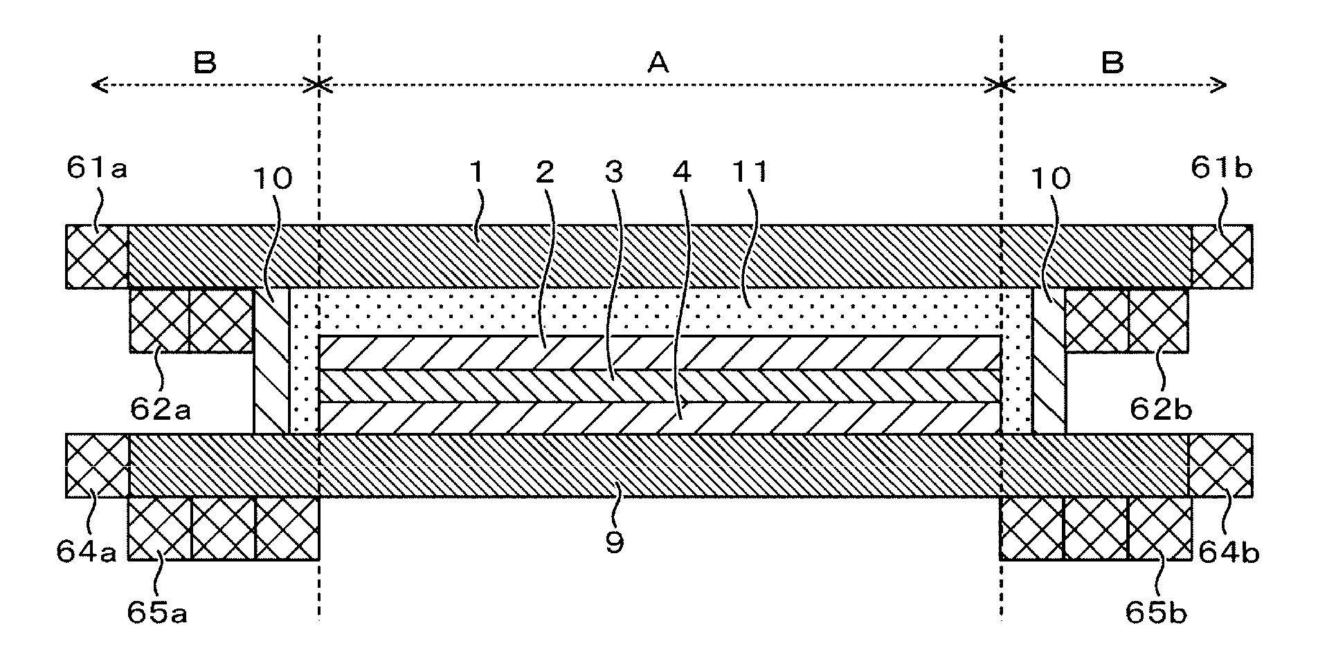
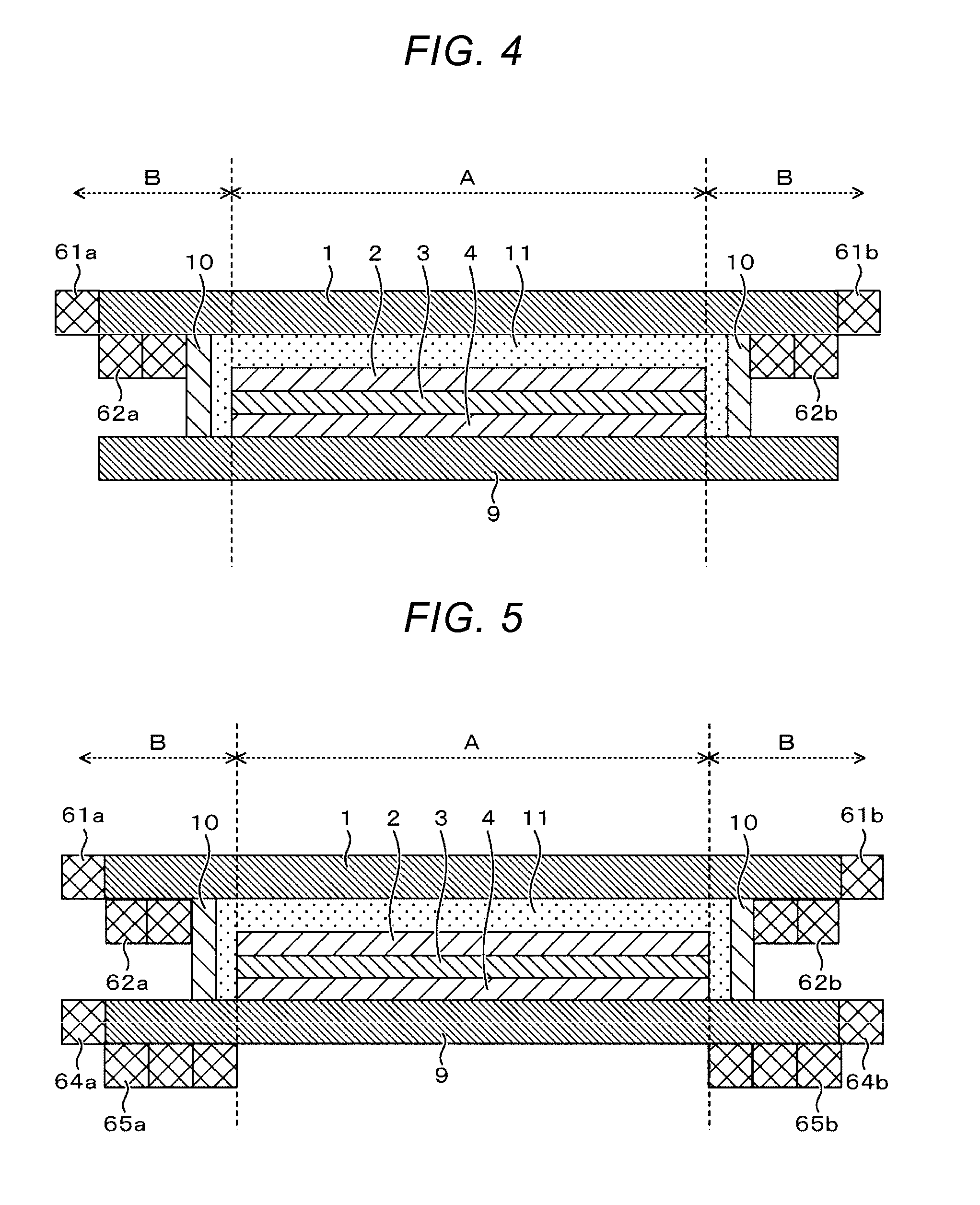
[0050]ITO was deposited by sputtering on a front substrate 1 made of glass with a thickness of 1.1 mm. The resulting glass substrate was cut into a 50-mm square, and the ITO was etched into strips with a width of 2 mm, whereby a transparent electrode 2 (anode) was formed. This front substrate 1 having the transparent electrode 2 formed thereon was ultrasonically cleaned for 15 minutes in acetone, pure water, and isopropyl alcohol, followed by drying and UV-ozone cleaning.

[0051]Subsequently, this front substrate 1 having the transparent electrode 2 formed thereon was placed in a vacuum deposition device, and under a reduced pressure of 1.33×10⁻⁴ Pa, 4,4′-bis[N-(naphthyl)-N-phenylamino]biphenyl (α-NPD, manufactured by Dojindo Laboratories Co., Ltd.) was deposited to a thickness of 30 nm at a deposition rate of 0.1 to 0.2 nm / s, whereby a hole transport layer was formed on the transparent electrode 2. Then, an organic light-emitting layer 3 was formed on the hole transport layer by lami...

example 2

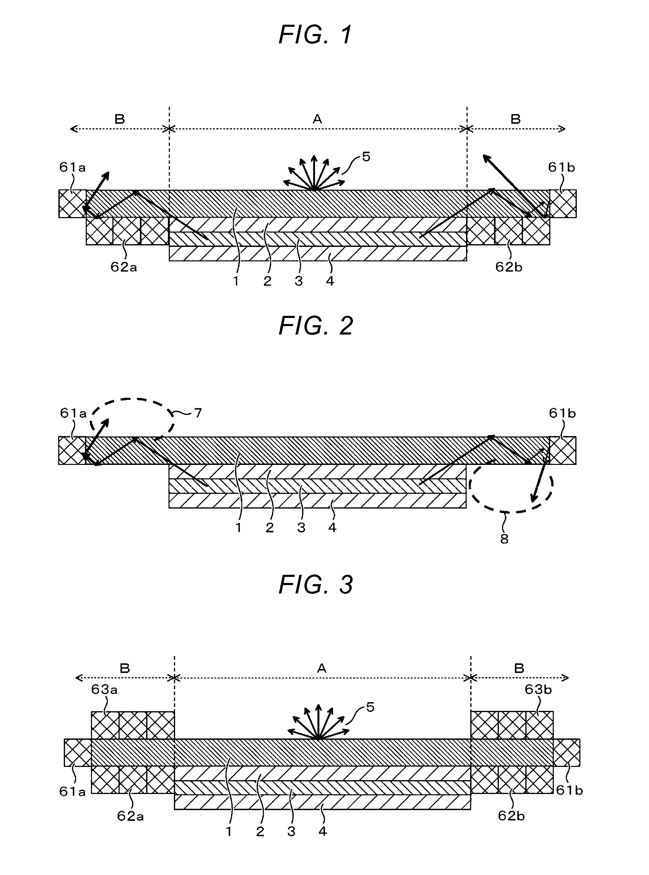
[0054]A sample corresponding to FIG. 3 was produced by forming diffuse reflectors 63a and 63b in non-light-emitting regions on the light exit surface side of the front substrate 1 of the organic light-emitting device produced in Example 1 using the same material as in Example 1.

example 3

[0055]In place of the front substrate 1 of the organic light-emitting device produced in Example 1, a substrate having a refractive index (nd) at a wavelength of 587.6 nm of 1.6 was used. Specifically, a high-refractive index glass substrate “K-PSK300” manufactured by Sumita Optical Glass Inc. was used. The other configuration was the same as that in Example 1.


PUM


Abstract

An object of the present invention is to provide an organic light-emitting device, wherein light trapped in a substrate due to total reflection at the interface between air and a substrate is efficiently extracted to the air side.
The organic light-emitting device includes: a transparent electrode; a counter electrode; a light-emitting layer interposed between the transparent electrode and the counter electrode; a front substrate which allows light from the light-emitting layer to exit to the outside from a surface of the front substrate on the opposite side to the light-emitting layer side; and a diffuse reflector which reflects light from the light-emitting layer, wherein the diffuse reflector is provided on a side surface of the front substrate and at a given position on a surface thereof.

Description

BACKGROUND OF THE INVENTION[0001]1. Field of the Invention[0002]The present invention relates to an organic light-emitting device and a light source device using an organic light-emitting device.[0003]2. Background Art[0004]As a related art, Patent document 1 (JP-A-2004-146121) discloses the following technique. That is, the technique aims to provide an organic electroluminescent device in which the leakage of light guided in a transparent substrate from a side surface of a transparent substrate and the extinction of the light inside the device can be prevented, and the light extraction efficiency is high. The technique relates to an organic electroluminescent device which is formed by providing an organic light-emitting layer between two electrodes and has a light-emitting section that allows the organic light-emitting layer to emit light by applying a voltage between the two electrodes. The organic electroluminescent device is configured such that a transparent electrode among the...

Claims


Application Information

Patent Timeline
Patent Type & Authority Applications(United States)
IPC IPC(8): H01L51/52
CPCH01L51/524H01L51/5271H01L51/5246H10K50/841H10K50/856H10K50/8426
Inventor NOBUKI, SHUNICHIROISHIHARA, SHINGO
Owner HITACHI LTD
Why Eureka
Try Eureka