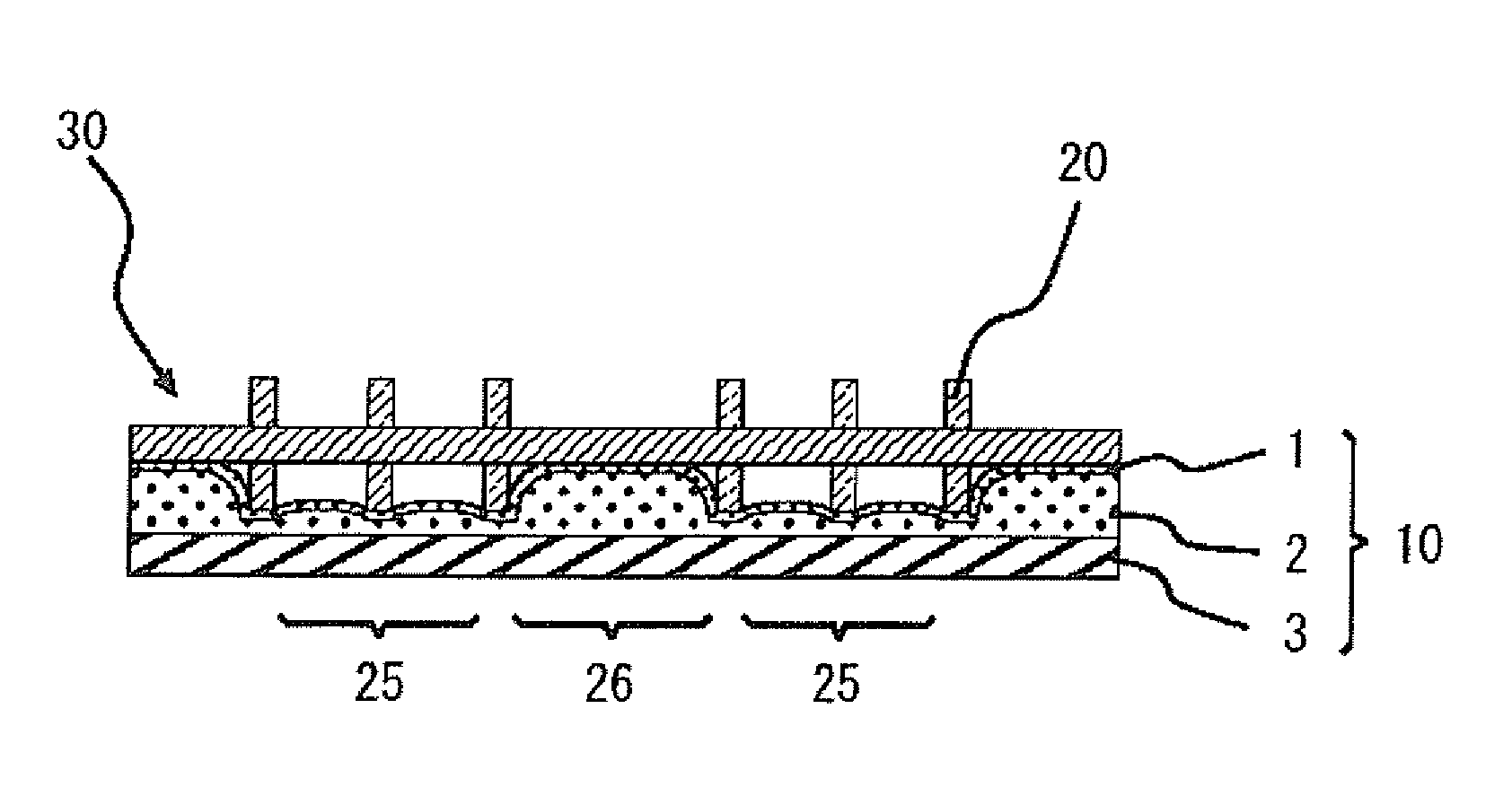
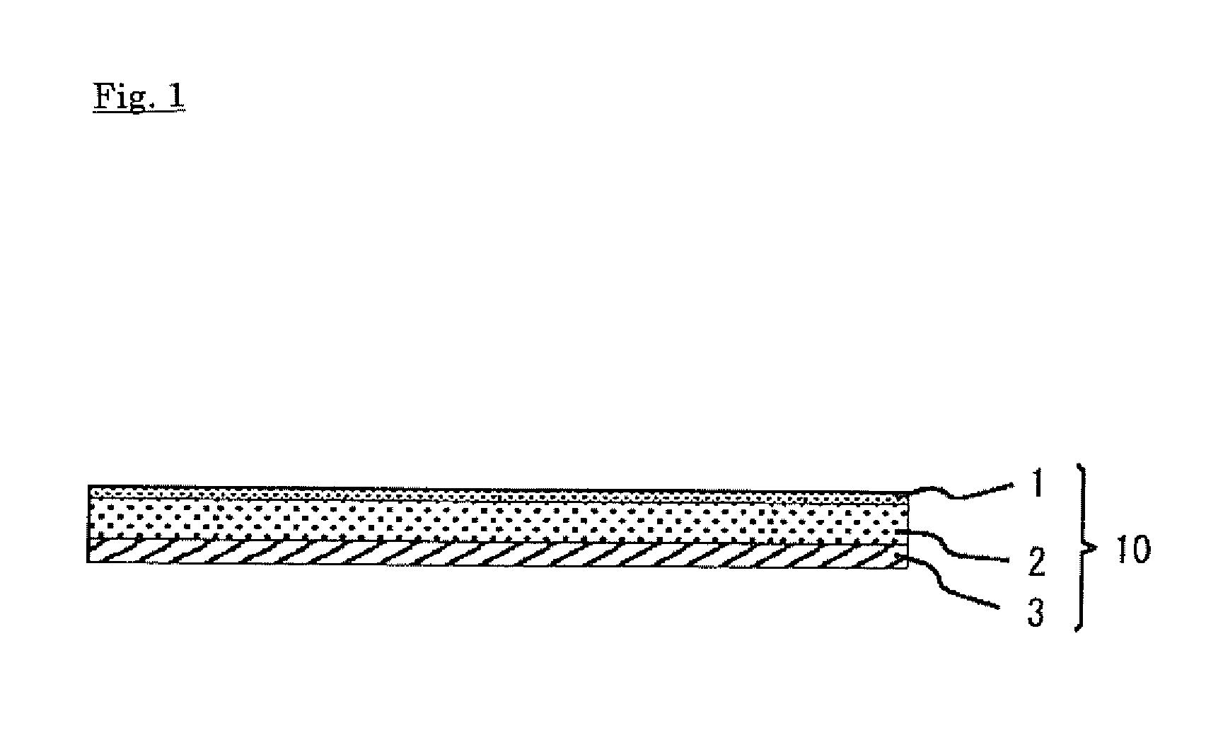
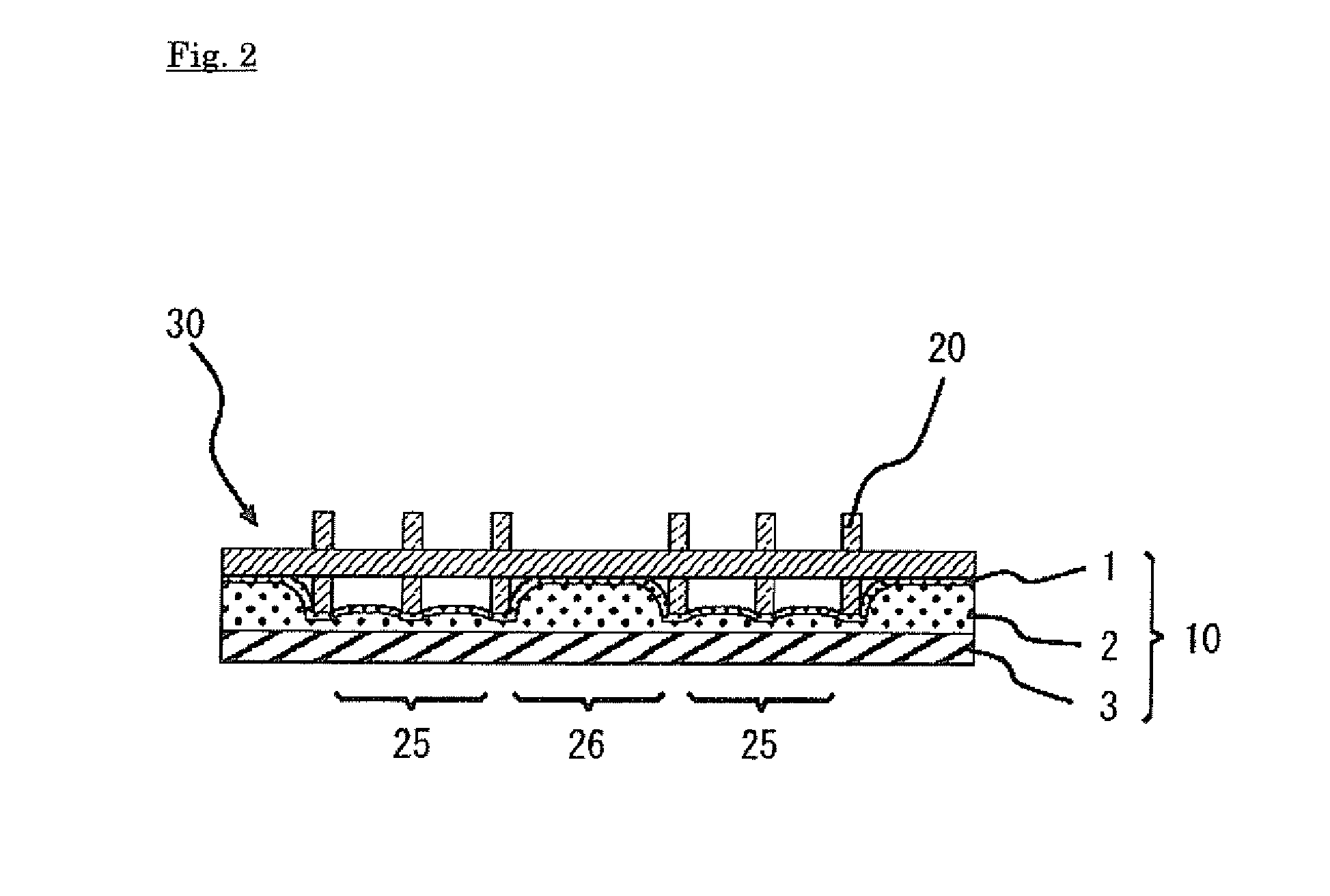
Dicing Sheet and a Production Method of a Semiconductor Chip
a technology of dicing sheet and production method, which is applied in the direction of solid-state devices, transportation and packaging, layered products, etc., can solve the problems of easy chipping, not necessarily completely eliminating the possibility of remaining residues, and the reliability of the semiconductor chip may decline, so as to prevent water intrusion, prevent chipping, and prevent the effect of dicing
- Summary
- Abstract
- Description
- Claims
- Application Information
AI Technical Summary
Benefits of technology
Problems solved by technology
Method used
Image

Examples
example 1
[The Production of the Adhesive Composition]
[0088]100 parts by weight of the energy ray curable adhesive polymer (the weight average molecular weight: 600000) was obtained by reacting the acrylic adhesive polymer obtained by reacting the butylacrylate / methyl(meth)acrylate / 2-hydroxyethylacrylate=62 / 10 / 28 (weight ratio) and 30.2 g of methacryloyloxyethylisocyanate (MOI) per 100 g of said acrylic adhesive polymer (80 mol per 100 mol of 2-hydroxyethylacrylate unit of the acrylic adhesive polymer), 3 parts by weight of photopolymerization initiator (α-hydroxycyclohexylphenylketone (IRGACURE 184 made by CIBA Speciality Chemicals)), and 8.6 parts by weight of the crosslinking agent (polyvalent isocyanate compound (CORONATE L made by NIPPON POLYURETHANE INDUSTRY Co., Ltd.) were mixed in the solvent thereby obtained the adhesive composition. Note that, weight average molecular weight is a value obtained by using a commercially available molecular weight measuring device (the product name: “H...
example 2
[0094]The dicing sheet was obtained as same as the example 1 except for making the thickness of the intermediate layer to 20 μm, and carried out each evaluation. The results are shown in Table 1.
example 3
[0095]The dicing sheet was obtained as same as the example 1 except for using the ethylene methacrylic acid copolymer film having thickness of 60 μm as the base, and carried out each evaluation. The results are shown in Table 1.
PUM
 Abstract
Description
Claims
Application Information
 - R&D
- Intellectual Property
- Life Sciences
- Materials
- Tech Scout
- Unparalleled Data Quality
- Higher Quality Content
- 60% Fewer Hallucinations
Browse by: Latest US Patents, China's latest patents, Technical Efficacy Thesaurus, Application Domain, Technology Topic, Popular Technical Reports.
© 2025 PatSnap. All rights reserved.Legal|Privacy policy|Modern Slavery Act Transparency Statement|Sitemap|About US| Contact US: help@patsnap.com