Structure for High-Speed Signal Integrity in Semiconductor Package with Single-Metal-Layer Substrate

Active Publication Date: 2013-05-30
TEXAS INSTR INC
View PDF0 Cites 17 Cited by
  • Summary
  • Abstract
  • Description
  • Claims
  • Application Information

AI Technical Summary

Benefits of technology

[0009]Applicants further recognized that for high frequency operation of a transmitter/receiver cell, the differential pairs need to have tight coupling within the pair, but the differential pairs need to be placed next to one another. This placement causes signific

Problems solved by technology

In view of these trends, applicants saw that the existence of metal-filled vias between the metal multi-layers is severely taxing the mismatch budget of high-speed signal packages.
The reasons can be found in the inherent imperfections of the vias: Chances for dimensional mismatch of the signal paths are necessarily increased by the additional drilling of the via holes, the electroplating of the v

Method used


Image

  • Structure for High-Speed Signal Integrity in Semiconductor Package with Single-Metal-Layer Substrate
  • Structure for High-Speed Signal Integrity in Semiconductor Package with Single-Metal-Layer Substrate
  • Structure for High-Speed Signal Integrity in Semiconductor Package with Single-Metal-Layer Substrate

Examples


Embodiment Construction

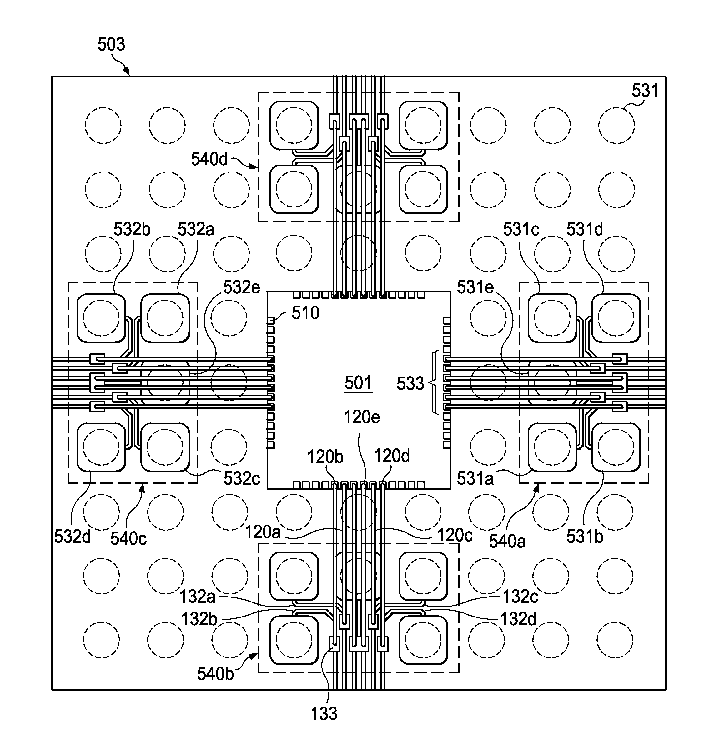
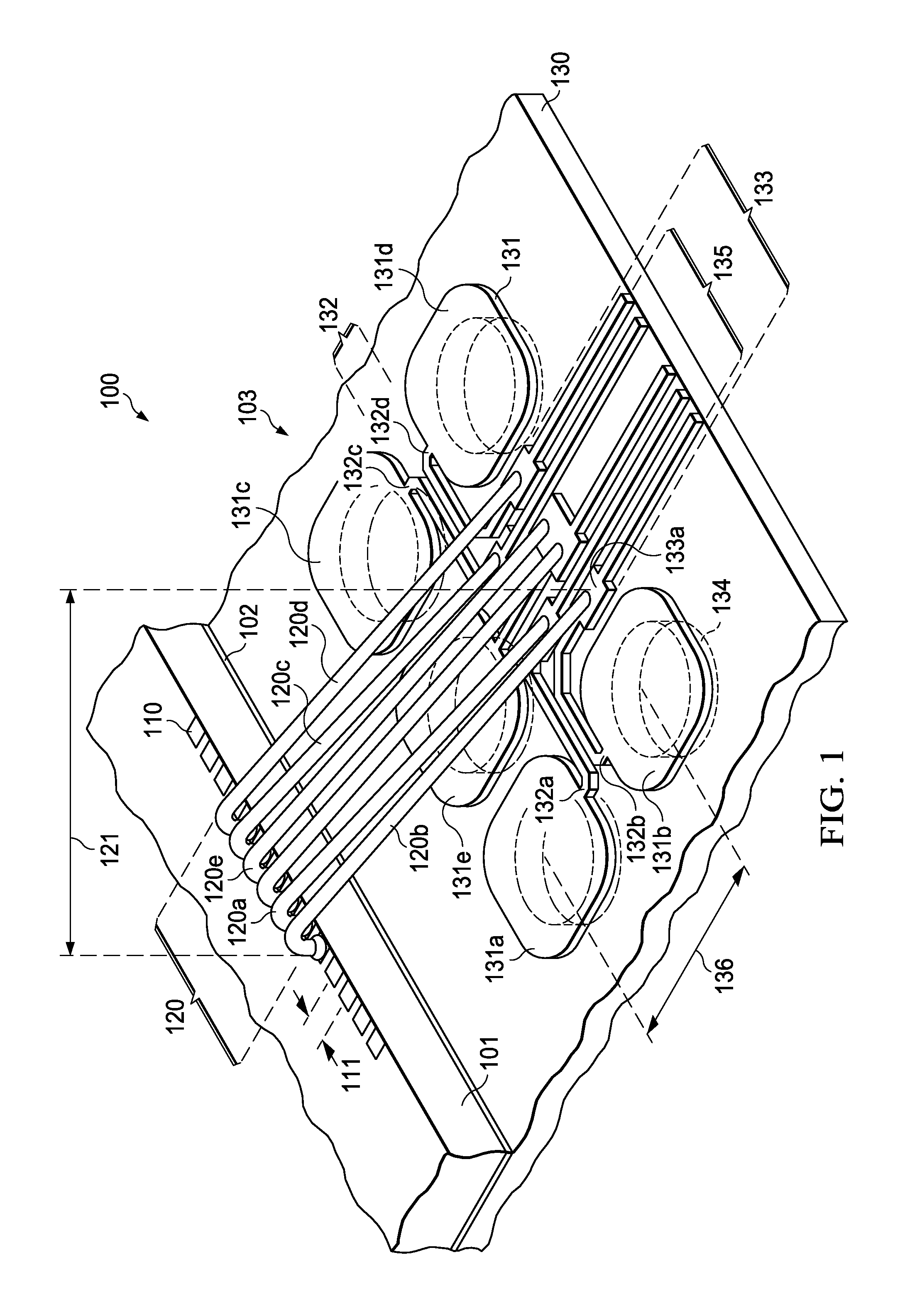
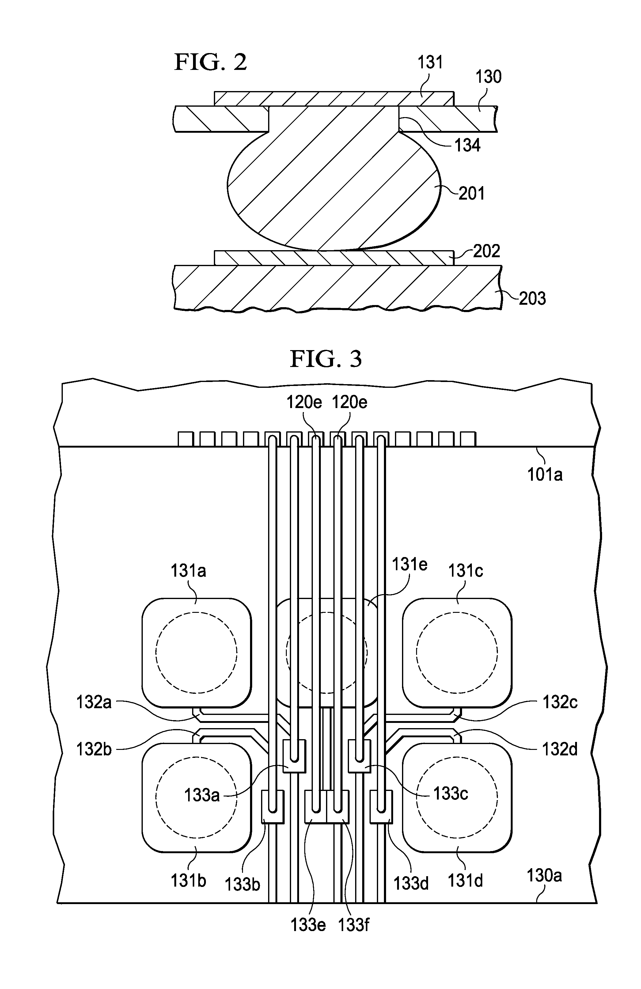
[0018]FIG. 1 illustrates an exemplary transmitter / receiver cell, generally designated 100, for conducting high-frequency signals with integrity in a semiconductor package according to an embodiment of the invention. A semiconductor chip 101 is attached to a substrate 103 by means of an adhesive attachment layer 102 (layer thickness approximately 20 μm). In the example of FIG. 1, the chip may have a thickness of about 280 μm; in other embodiments, the thickness may be greater or smaller.

[0019]Located near an edge, chip 101 has a plurality of metal bond pads 110 suitable of affixing bonds of a metal wire. In the example of FIG. 1, an individual wire of the wire plurality 120 may have a diameter between about 20 and 30 μm, which produces a free air ball of about 30 to 50 μm and a squashed ball of about 30 to 60 μm. While bond pads 110 in FIG. 1 are depicted as being arrayed in a linear and orderly row with a pitch center-to-center of about 60 μm, other embodiments may have a staggered ...


PUM


Abstract

A semiconductor chip (101) with bond pads (110) on a substrate (103) with rows and columns of regularly pitched metal contact pads (131). A zone comprises a first pair (131a, 131b) and a parallel second pair (131c, 131d) of contact pads, and a single contact pad (131e) for ground potential; staggered pairs of stitch pads (133) connected to respective pairs of adjacent contact pads by parallel and equal-length traces (132a, 132b, etc.). Parallel and equal-length bonding wires (120a, 120b, etc.) connect bond pad pairs to stitch pad pairs, forming differential pairs of parallel and equal-length conductor lines. Two differential pairs in parallel and symmetrical position form a transmitter/receiver cell for conducting high-frequency signals.

Description

FIELD OF THE INVENTION[0001]The present invention is related in general to the field of semiconductor devices and processes and more specifically to configuration and fabrication method of a structure for high-speed signal integrity in semiconductor packages with single-metal-layer substrate and wire bonds.DESCRIPTION OF RELATED ART[0002]Semiconductor devices typically include an integrated circuit (IC) chip and a substrate integrated with the chip within a package encapsulating the device. In order for a modern semiconductor device to function as intended, it is required that any pair of differential signals that propagates through the device be matched, within prescribed limits, with regard to relative magnitude and relative phase angle of the signal waves.[0003]For the design of an integrated circuit (IC) chip with regard to differential signals, the building blocks may employ circuit components, which have been matched by interdigitating critical layout for components, such as t...

Claims


Application Information

Patent Timeline
IPC IPC(8): H01L23/49
CPCH01L24/49H01L2224/49113H01L24/06H01L2224/45015H01L2924/15311H01L2224/48465H01L23/49816H01L2924/3011H01L2224/73265H01L2224/32225H01L2224/06155H01L2224/04042H01L2223/6611H01L24/73H01L24/48H01L24/45H01L24/32H01L23/66H01L2224/49433H01L2224/49175H01L2224/48227H01L2924/20752H01L2924/00H01L2924/00012H01L23/49838H01L2924/3025H01L2224/05554H01L2224/451H01L2924/30111H01L2924/181H01L2924/00014H01L2224/05599
Inventor HOWARD, GREGORY E.ROMIG, MATTHEW D.MILLERON, MARIE-SOLANGE ANNEMUKHERJEE, SOUVIK
Owner TEXAS INSTR INC
Why Eureka
Try Eureka