Methods for selective etching of a multi-layer substrate

a multi-layer substrate and selective etching technology, applied in the direction of basic electric elements, electrical apparatus, semiconductor devices, etc., can solve the problems of low resistance metal oxide film not being able to form a reliable nonvolatile memory device, the resistance of low resistance metal oxide film is often insufficient to meet the needs of traditional nonvolatile memory technology, and the resistance of these films and the ratio of high-to-low resistance states are often insufficient to meet the needs of practical nonvolatil

Inactive Publication Date: 2013-05-30
INTERMOLECULAR
View PDF4 Cites 29 Cited by
  • Summary
  • Abstract
  • Description
  • Claims
  • Application Information

AI Technical Summary

Benefits of technology

[0012]In some embodiments, the present invention discloses a combination of selective wet and dry etching processes to pattern the metal oxide stack. The processes comprise a physical sputtering to etch a capping layer of platinum or tungsten, which can be highly selective against a patterned photoresist layer and the top electrode materials of titanium or tantalum nitride. The top electrode of TiN layer then can be selectively wet etched using Standard Clean 1 (SC-1, comprising a mixture of NH4OH and H2O2), stopping on the metal oxide layer of HfO2 or ZrO2. A wet etch solution comprising dilute HF and HCl can be effective in etching the metal oxide layer of HfO2 or ZrO2 with minimum damage to the isolation layer of SiO2 and stopping on the polysilicon substrate.
[0014]In some embodiments, the present invention discloses a combination of selective wet etching processes to pattern the metal oxide stack. The processes comprise a Standard Clean 1 (SC-1, comprising a mixture of NH4OH and H2O2) to selectively etch a cap layer of tungsten, together with a top electrode layer of titanium nitride or tantalum nitride, stopping on the metal oxide layer of HfO2 or ZrO2. A wet etch solution comprising dilute HF and HCl can be effective in etching the metal oxide layer of HfO2 or ZrO2 with high selectivity to isolation layer of SiO2 and stopping on the polysilicon substrate with minimum damage.

Problems solved by technology

However, as device dimensions shrink, scaling issues are posing challenges for traditional nonvolatile memory technology.
Although metal oxide films such as these exhibit bistability, the resistance of these films and the ratio of the high-to-low resistance states are often insufficient to be of use within a practical nonvolatile memory device.
Therefore, a low resistance metal oxide film may not form a reliable nonvolatile memory device.
For example, in a nonvolatile memory that has conductive lines formed of a relatively high resistance metal such as tungsten, the resistance of the conductive lines may overwhelm the resistance of the metal oxide resistive switching element.
Therefore, the state of the bistable metal oxide resistive switching element may be difficult or impossible to sense.
This can result in etched features that have smaller line widths than those of the patterning images.
The poor selectivity can cause under or over etch issues and cross-contamination / residues remaining after the etch process.

Method used


Image

  • Methods for selective etching of a multi-layer substrate
  • Methods for selective etching of a multi-layer substrate
  • Methods for selective etching of a multi-layer substrate

Examples


Embodiment Construction

[0031]A detailed description of one or more embodiments is provided below along with accompanying figures. The detailed description is provided in connection with such embodiments, but is not limited to any particular example. The scope is limited only by the claims and numerous alternatives, modifications, and equivalents are encompassed. Numerous specific details are set forth in the following description in order to provide a thorough understanding. These details are provided for the purpose of example and the described techniques may be practiced according to the claims without some or all of these specific details. For the purpose of clarity, technical material that is known in the technical fields related to the embodiments has not been described in detail to avoid unnecessarily obscuring the description.

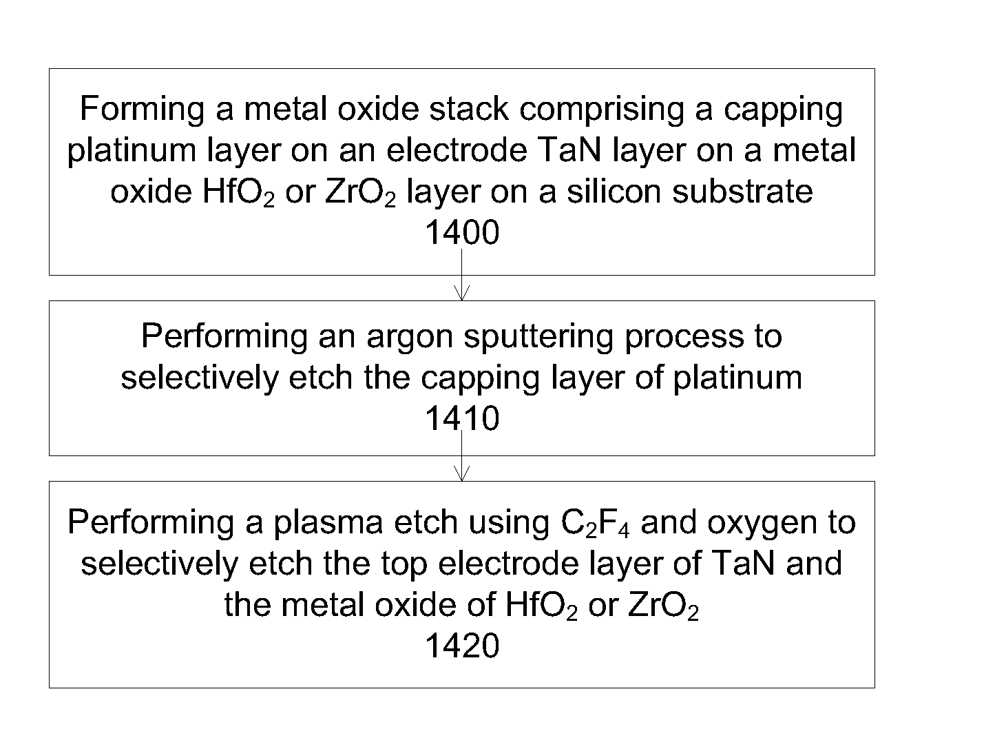
[0032]In some embodiments, the present invention discloses a selective etch method for patterning a multilayer ReRAM stack. High selectivity for different layers of the multil...


PUM


Abstract

A method is disclosed for the selective etching of a multi-layer metal oxide stack comprising a platinum or tungsten layer on a TiN layer on an HfO2 or ZrO2 layer on a silicon substrate. In some embodiments, the method comprises a physical sputter process to selectively etch the platinum layer, followed by a first wet etch using a mixture of NH4OH and H2O2 to selectively etch the TiN layer, and a second wet etch using a dilute mixture of HF and HCl to selectively etch the HfO2 or ZrO2 layer.

Description

FIELD OF THE INVENTION[0001]The present invention relates generally to a process for etching a multi-layer substrate, and more particularly to a selective etching process for metal oxide stacks.BACKGROUND OF THE INVENTION[0002]Nonvolatile memory elements are used in systems in which persistent storage is required. For example, digital cameras use nonvolatile memory cards to store images and digital music players use nonvolatile memory to store audio data. Nonvolatile memory is also used to persistently store data in computer environments. Nonvolatile memory is often formed using electrically-erasable programmable read only memory (EPROM) technology. This type of nonvolatile memory contains floating gate transistors that can be selectively programmed or erased by application of suitable voltages to their terminals.[0003]As fabrication techniques improve, it is becoming possible to fabricate nonvolatile memory elements with increasingly smaller dimensions. However, as device dimension...

Claims


Application Information

Patent Timeline
Patent Type & Authority Applications(United States)
IPC IPC(8): H01L21/3065
CPCH01L21/31116H01L21/32134H01L45/08H01L45/1233H01L45/146H01L45/16H01L27/2409H01L27/2463H01L21/3065H01L45/1253H01L45/1675H10B63/20H10B63/80H10N70/24H10N70/826H10N70/8833H10N70/063H10N70/011H10N70/841
Inventor TONG, JINHONGFULGENCIO, FREDERICKSHAO, SHOUQIAN
Owner INTERMOLECULAR
Why Eureka
Try Eureka