Laser Illuminator System

a laser and illumination technology, applied in the field of laser illumination, can solve the problems of high electrical energy requirement for operation, large footprint of mode-locked lasers, and complex cooling peripheral equipment, and achieve the effects of high thermal conductivity, rapid heat dissipation, and high thermal conductivity

Inactive Publication Date: 2013-06-27
PRINCETON OPTRONICS
View PDF6 Cites 191 Cited by
  • Summary
  • Abstract
  • Description
  • Claims
  • Application Information

AI Technical Summary

Benefits of technology

[0020]In one embodiment of a high power illuminator, a VCSEL array is bonded to large area bonding pads located on one surface of a thermal submount. The thermal submount is constructed from a high thermal conductivity material such that heat generated in the VCSEL array is rapidly dissipated away to avoid thermal degradation during high power operation. In a variant embodiment the large area bonding pads are wrapped around respective edges of the thermal submount and connected to a second set of large area bonding pads located on an opposite surface underside of the thermal submount. The thermal submount is designed to be directly bonded to a heat sink, a PCB or a specially designed PCB including a heat sink region, such that the VCSEL array is in good thermal contact with a heat sink for rapid heat dissipation from the VCSEL array.
[0021]In an alternate embodiment, the thermal submount further includes a plurality of via holes located between a top surface and an opposing bottom surface of the submount. The via holes are coated and / or filled with a material that has a high thermal conductivity as well as a high electrical conductivity so as to provide good thermal and electrical contact between corresponding large bonding pads located on the opposing surfaces of the thermal submount. The thermal submount is designed to be directly bonded to a heat sink, a PCB or a specially designed PCB including a heat sink region, such that the VCSEL array is in good thermal contact with a heat sink for rapid heat dissipation from the VCSEL array.

Problems solved by technology

However, current cost of devices is rather high for other emerging applications particularly in consumer electronics and optics and / or in portable devices.
However Q-switched or mode-locked lasers have large footprint, require high electrical energy requirement for operation and elaborate cooling peripheral equipment.
It is noted that the electrical contacts are on only one side of the subassembly and do not provide a connection to the underside for direct surface mount attaching to a PCB.
The subassembly is only suitable for single devices and not designed for VCSEL arrays.
Furthermore, there is no provision in the design for thermal conduction of heat away from the VCSEL arrays particularly encountered in high power operation.
And while the submount has high speed, it does not provide connections from the top surface to the underneath surface of the submount.
It is not suited for high speed connection to a printed circuit board (PCB) and it does not support low thermal resistance path to a heat sink.
Each pad contains only one via per pad and therefore does not provide sufficiently low thermal resistance path which is particularly needed for high current / power operation.
In addition, the vias and pads do not provide a low inductance path which is necessary for driving the VCSEL at high current and high speed, in particular for a high power VCSEL array where a plurality of VCSELs operate together.
However, the disclosure does not describe packing laser or detector arrays in that fashion.
More specifically, the submount described therein comprises specially designed and fabricated VCSEL arrays with raised mesa structures and additional non emitting shorting mesas to provide the means for connecting to the high speed submount and proving heat sinking However, the submount is not electrically bonded to a high speed PCB including mechanically bonding to a heat sink for providing efficient cooling for high power operation.

Method used


Image

  • Laser Illuminator System
  • Laser Illuminator System
  • Laser Illuminator System

Examples


Embodiment Construction

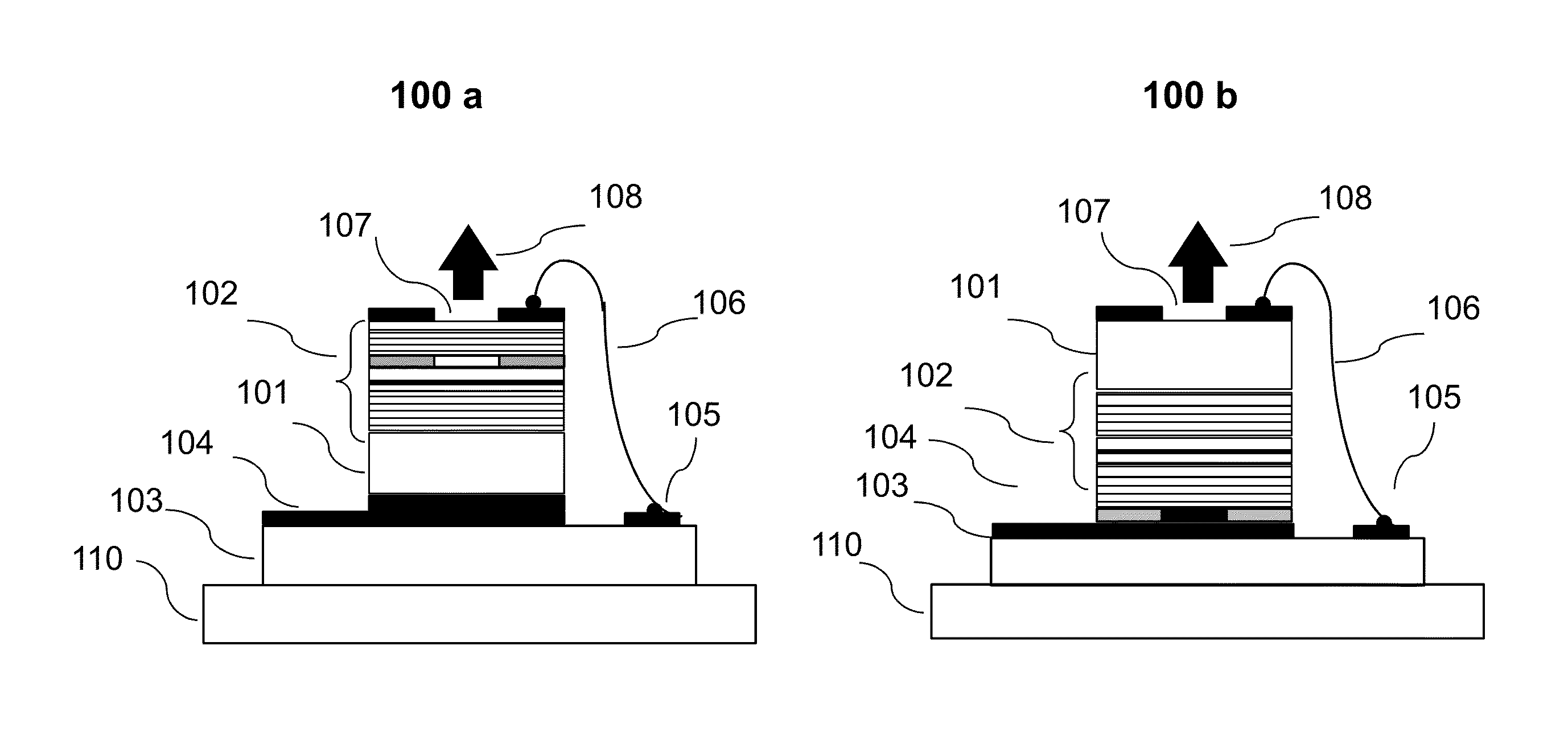
[0037]For clarity and ease of discussion, each drawing figure shows a particular aspect or a combination of few aspects that may be implemented in an embodiment either alone or, in combination with one or more aspects shown in other embodiments. An element not shown in any particular embodiment is not be construed as precluded from the embodiment unless stated otherwise. Different aspects presented separately in the preferred embodiments are intended to provide a broader perspective of the invention. Different combinations and sub-combinations of various aspects that may occur to those skilled in the art, still fall within the broader framework of the detailed description of the invention presented in the following sections of the written description.

Single VCSEL Module:

[0038]A laser illuminator may be configured using a single high power VCSEL. In one embodiment, an optical module is configured using a single VCSEL as shown in FIG. 1. Principles illustrated through this exemplary e...


PUM


Abstract

An optical illuminator using Vertical Cavity Surface Emitting Laser (VCSEL) is disclosed. Optical modules configured using single VCSEL and VCSEL arrays bonded to a thermal submount to conduct heat away from the VCSEL array, are suited for high power and high speed operation. High speed optical modules are configured using single VCSEL or VCSEL arrays connected to a high speed electronic module on a common thermal submount or on a common Printed Circuit Board (PCB) platform including transmission lines. The electronic module provides low inductance current drive and control functions to operate the VCSEL and VCSEL array. VCSEL apertures are designed for a desired beam shape. Additional beam shaping elements are provided for VCSELs or VCSEL arrays, for desired output beam shapes and/or emission patterns. VCSEL arrays may be operated in continuous wave (CW) or pulse operation modes in a programmable fashion using a built-in or an external controller.

Description

BACKGROUND OF THE INVENTION[0001]1. Field of the Invention[0002]This invention relates to the field of laser illumination and in particular, to an illuminator system including single Vertical Cavity Surface Emitting Laser (VCSEL) and arrays of VCSELs.[0003]2. Description of the Related Arts[0004]Laser illumination sources have diverse applications depending upon different operating modes such as, continuous wave (CW), Quasi Continuous Wave (QCW) or pulsed operation. To name just a few, laser illumination is widely used in the field of surveillance imaging, recording images of objects moving at high speed, gesture recognition, time of flight illumination for three dimensional (3D) imaging, etc. Currently, laser devices operating in the visible as well as in the Infra-red (IR) region of the electromagnetic spectrum are readily available. However, current cost of devices is rather high for other emerging applications particularly in consumer electronics and optics and / or in portable de...

Claims


Application Information

Patent Timeline
Patent Type & Authority Applications(United States)
IPC IPC(8): H01S3/04H01S3/00H01S5/183H01S5/42
CPCH01S5/02228H01S5/02248H01L2224/48091H01L2224/4848H01L2224/48465H01S2301/18H01S5/423H01S5/18311H01S5/02276H01S5/02288H01S5/02469H01S5/02476H01S5/06226H01L2924/00014H01L2924/00H01S5/02234H01S5/02253H01S5/02325H01S5/02345
Inventor SEURIN, JEAN F.GHOSH, CHUNI L.WANG, QING
Owner PRINCETON OPTRONICS
Why Eureka
Try Eureka