Soi lateral mosfet devices

a technology of lateral mosfet and semiconductors, applied in the direction of semiconductor devices, basic electric elements, electrical equipment, etc., can solve the problems of increasing the chip area and cost of devices (or circuits), increasing power loss and switching speed, and reducing the permittivity. , to achieve the effect of enhancing the electric field strength in the dielectric trench, reducing the permittivity, and improving the breakdown voltag

Inactive Publication Date: 2013-08-01
UNIV OF ELECTRONICS SCI & TECH OF CHINA
View PDF1 Cites 17 Cited by
  • Summary
  • Abstract
  • Description
  • Claims
  • Application Information

AI Technical Summary

Benefits of technology

[0024]Silicon dioxide is generally used as dielectric for Si semiconductor based on the existed process. The relative permittivity of 3.9 for SiO2 is lower than 11.9 for Si, thereby, the electric field strength in the dielectric trench is enhanced and breakdown voltage is improved. The dielectric which has a lower permittivity than that of SiO2 and a higher critical electric filed than three times of Si can further improve the BV.
[0025]The material of said active layer is Si, the gate dielectric is SiO2, or the dielectric with a higher permittivity than that of SiO2. Said gate dielectric includes but does not restrict to Si3N4, Al2O3, AlN or HfO2. Said gate dielectric with a higher permittivity can enhance the control of gate voltage to gate charges and enhance the transconductance. Said gate dielectric can be thicker at the same gate structure MIS (Metal—Insulator—Semiconductor, gate electrode—gate dielectric—the semiconductor under the gate dielectric forming the MIS structure) capacitance, which reduces the tunnel current and avoids tunnel breakdown, and thus enhances the stability as well as reliability of the device or chips.
[0026]Said dielectric buried layer is SiO2 or the dielectric with a lower permittivity than that of SiO2 and a higher critical electric field than three times of Si and said active layer is Si material. And said dielectric buried layer material includes but does not restrict to SiOF, Carbon doped Oxide (CDO) or SiCOF. Said dielectric buried layer using dielectric with a lower permittivity can enhance the electric field of the dielectric buried layer, so BV is increased.
[0027]The advantages of the present invention are as follows: ① In blocking state, in the lateral direction, the dielectric in the dielectric trench between drain region and source region b shares breakdown voltage. The electric field strength in dielectric trench is far higher than that of the active layer because of the lower permittivity of dielectric (e.g. SiO2) than that of the semiconductor active layer (e.g. Si). In the vertical direction, the trench gate and the dielectric trench enhance multi-dimensional depletion in the active layer; both of them greatly improve breakdown voltage at the same pitch. On the other hand, at the same breakdown voltage, the length of drift region and pitch significantly decrease, resulting in the reduced on-resistance (Ron) and power loss. Both the cost and the scale of chips could therefore be declined. ② The dielectric trench folds the drift region in the vertical direction, and this shrinks the device pitch, leading to a reduced specific on-resistance and a low chip cost, increasing switching speed. ③ In the on-state condition, the trench gate extended to the dielectric buried layer widens the effective conductive region in the vertical direction in the drift region and reduces the Ron and power loss; Furthermore, the buried gate further increases the channel and current densities, resulting in a reduced power loss. ④ In high voltage blocking condition, the gate dielectric extended to the interface over the dielectric buried layer terminates the high potential from the drain at the center of device within the trench gate, avoiding the influence of the high potential on the low-voltage circuits outside the trench gate. Thereby, the trench gate acts as a dielectric isolation trench, saving the area of the dielectric isolation trench, simplifying isolation process in conventional SOI high-voltage IC where the dielectric isolation trench is formed by a particular process and saving the chip cost. In short, present invention offers a lateral SOI MOSFET, which has advantages including high breakdown voltage, high speed, low power loss, low cost and miniaturization, and said lateral SOI MOSFET can be easily integrated with power IC.

Problems solved by technology

This makes device (or circuit) chip area and cost increase, and also it is adverse to miniaturization of chip.
The increase in Ron leads to an increase in power loss and decrease in switching speed.
It can be seen that the effect of this structure on reducing the drift region length and the specific on-resistance is limited.
For the BV>100V TLPM / D MOSFE, the effect on reducing the pitch will be weakened with the increasing thickness of the thicker sidewall oxide layer 32 at the lower half of trench; meanwhile, it become difficult to fabricate the drain- and the gate-electrode in one deep and narrow trench as the trench depth increases with an increasing breakdown voltage.
In these two structures, the drain- and the gate-electrode or the source- and the gate- electrode are required to fabricate in one trench, the process thereby becomes more difficult as BV increases (trench depth increases); moreover, the effect on reducing the pitch becomes weak with an increasing BV.
Its process thus is more complex.

Method used


Image

  • Soi lateral mosfet devices
  • Soi lateral mosfet devices
  • Soi lateral mosfet devices

Examples


embodiment 1

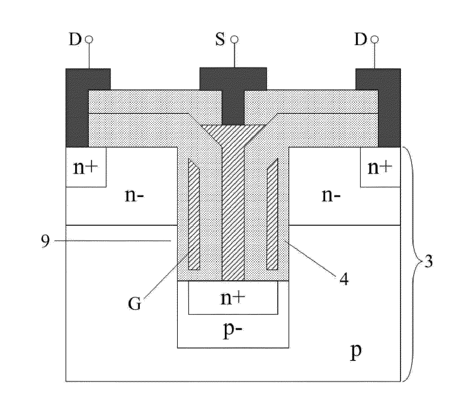
[0048]FIG. 5 shows the layout of the cell of a lateral SOI MOSFET with plane symmetry. The figure shown is in the xz plane, wherein the AA′ line is along the x direction, BB′ is along the z direction, and y is the vertical direction. Symmetric plane of the device is the yz plane through BB′ line. The layout in FIG. 5 includes such layers as dielectric trench 61, trench gate 8, and the metallic electrode layers: trench gate electrode 21, buried gate electrode 22, gate electrode G, source electrode S and drain electrode D. In this layout, the source region, drain region, trench gate 8, dielectric trench 61, buried gate, and other figures operating electrically are bars, and said drain electrode D is located in the center of the device, and said dielectric trench 61 is on both sides of drain electrode D; said source electrode S is in the outer side of dielectric trench 61; said trench gate 8 is located in the periphery of the device in order to isolate low voltage units from high volta...

embodiment 2

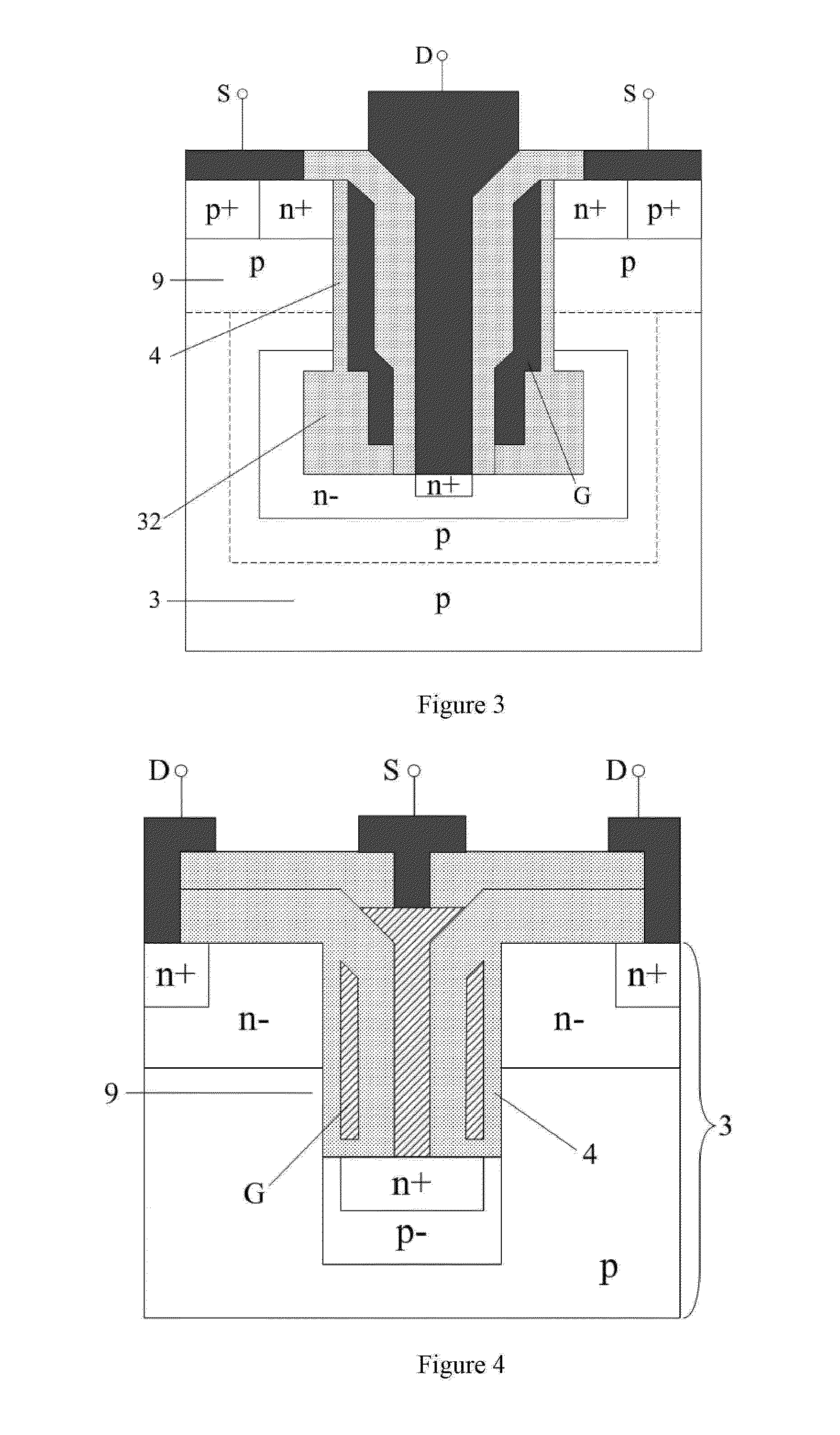
[0052]FIG. 8 shows another embodiment of the present invention, basically the same as the embodiment 1, except that n+ drain region in this embodiment is not in contact with said dielectric trench 61. Breakdown voltage increases to some extent while on-resistance increases slightly in this device, compared with that of the device structure in FIG. 7.

embodiment 3

[0053]In this case, the upper portion of the gate dielectric 4 is thinner than the lower portion of the gate dielectric, as showed in FIG. 9. This kind of trench gate 8 structure is better to improve breakdown voltage.


PUM


Abstract

The present invention relates to a semiconductor power device and power integrated circuits (ICs). The lateral SOI MOSFET in the present comprises a trench gate extended to the dielectric buried layer, one or multiple dielectric trenches in the drift region, and a buried gate in said dielectric trench. The permittivity of the dielectric in said dielectric trench is lower than that of said active layer. Firstly, said dielectric trench not only greatly improves breakdown voltage, but also reduces pitch size. Secondly, the trench gate widens the effective conductive region in the vertical direction. Thirdly, dual gates of said trench gate and buried gate increase channel and current densities. Thereby, specific on-resistance and the power loss are reduced. The device of the present invention has many advantages, such as high voltage, high speed, low power loss, low cost and ease of integration. The device in the present invention is particularly suitable for power integrated circuits and RF power integrated circuits.

Description

FIELD OF THE INVENTION[0001]The present invention relates to semiconductor power devices and power integrated circuits. It specifically relates to an SOI (Semiconductor On Insulator) lateral MOSFET (Metal-Oxide-Semiconductor Field-Effect-Transistor) in power integrated circuits or RF power integrated circuits, and more particularly relates to a high breakdown voltage and low power loss lateral MOSFET.BACKGROUND OF THE INVENTION[0002]An SOI structure consists of a top semiconductor layer, a substrate layer and a buried dielectric layer interposed between the top semiconductor layer and the substrate layer, where said top semiconductor layer is called active layer and said substrate layer is a semiconductor layer or dielectric layer. Semiconductor devices and circuits are formed in said active layer. In integrated circuits, high-voltage devices and low-voltage circuitry are isolated by isolation trench 30, while said active layer 3 and substrate layer 1 are isolated by dielectric laye...

Claims


Application Information

Patent Timeline
Patent Type & Authority Applications(United States)
IPC IPC(8): H01L29/78
CPCH01L27/1203H01L29/0619H01L29/0653H01L29/0696H01L29/4236H01L29/7827H01L29/4238H01L29/7809H01L29/7812H01L29/7813H01L29/42368
Inventor LUO, XIAORONGUDREA, FLORIN
Owner UNIV OF ELECTRONICS SCI & TECH OF CHINA
Why Eureka
Try Eureka