Iron based superconducting structures and methods for making the same

a superconducting structure and iron-based technology, applied in the direction of superconducting magnets/coils, instruments, magnetic bodies, etc., can solve the problems of limited application, difficult manufacturing steps, and inability to make superconducting tapes or wires for large-scale applications

Inactive Publication Date: 2013-08-01
BROOKHAVEN SCI ASSOCS
View PDF4 Cites 28 Cited by
  • Summary
  • Abstract
  • Description
  • Claims
  • Application Information

AI Technical Summary

Benefits of technology

[0014]In some embodiments, substrates comprise layers of buffer materials that improve the texture of the base to render it more suitable for formation of iron-based superconductor films thereupon. In some cases, a single layer of buffer material is used; in other cases, multiple layers of buffer materials are used.
[0017]In some embodiments, the superconducting thin films retain their inherent superconducting properties, including critical electrical currents, critical magnetic fields, and critical superconducting transition temperatures, and these properties are on par with those of films of similar composition and thickness to films grown on single-crystal substrates. In some cases, the superconducting properties of the thin films are better than those of bulk materials having the same composition.

Problems solved by technology

High field applications of superconductors have been dominated by Nb3Sn, a material which allows magnetic fields up to 20 T to be achieved at 4.2 K. However, Nb3Sn wires typically require a post-winding heat-treatment, which is a technically-challenging manufacturing step.
Although high temperature superconducting oxides (HTS) offer excellent superconducting properties, their characteristically high anisotropies and brittle textures, in addition to the high manufacturing costs, have limited their applications.
However, these films were made on crystalline substrates, which cannot be used to make superconducting tapes or wires for large scale applications.
However, due to the lattice mismatch between these substrates and those materials, it is very difficult to grow such films.

Method used


Image

  • Iron based superconducting structures and methods for making the same
  • Iron based superconducting structures and methods for making the same
  • Iron based superconducting structures and methods for making the same

Examples


example 1

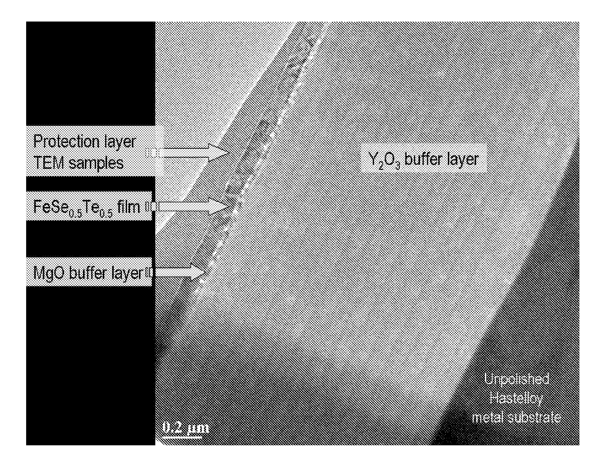
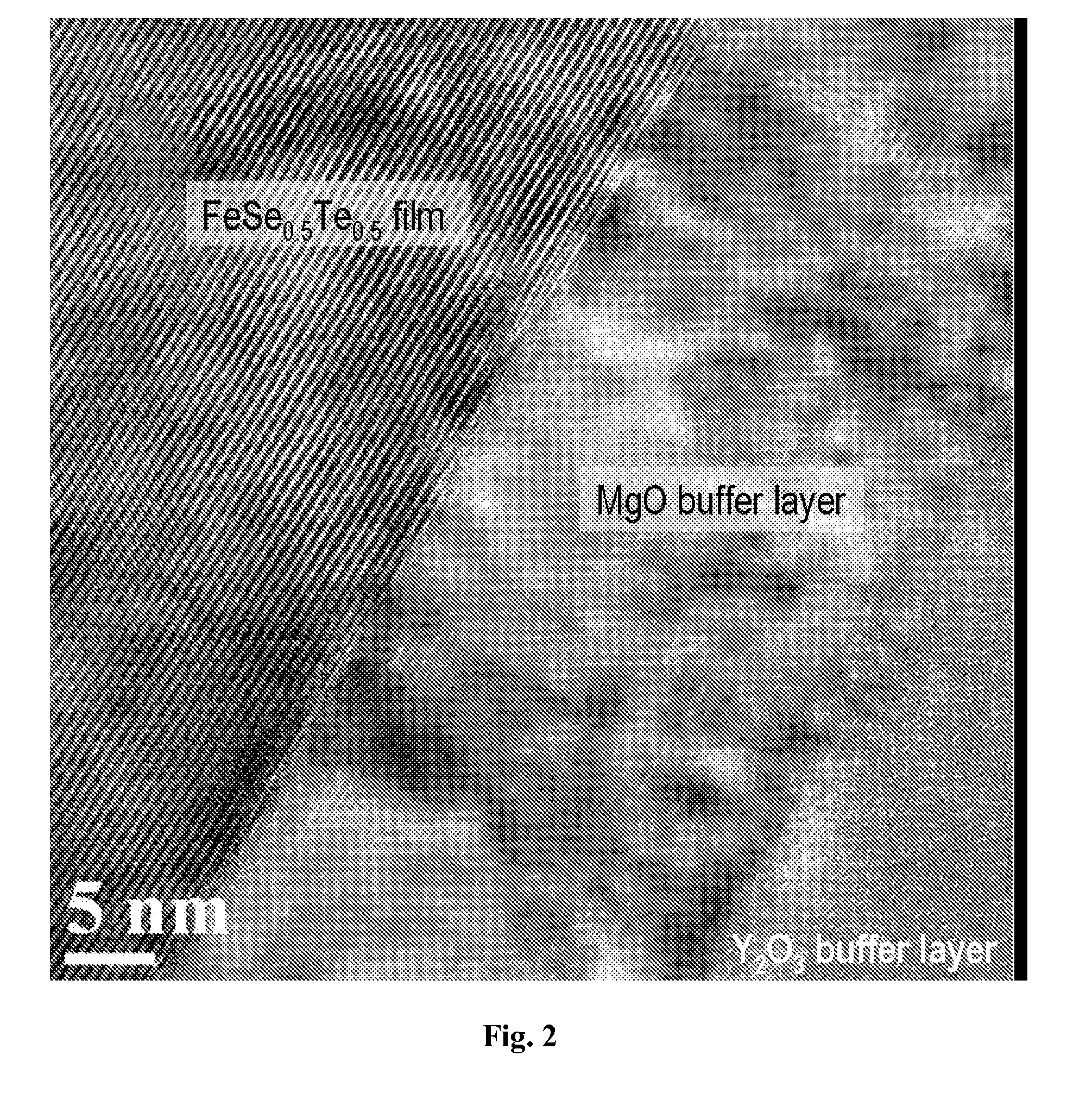
[0050]The films depicted in FIGS. 1 and 2 have a composition of FeSe0.5Te0.5 and were grown by pulsed laser deposition (PLD). The films were deposited on single crystalline LaAlO3 (LAO) substrates and buffered metal templates using a KrF excimer laser (wavelength: 248 nm) with an energy density of ˜3.0 J / cm2 and a repetition rate of 5 Hz. The substrate temperature was varied from 350° C. to 450° C. The time to deposit the 400-nm film was about 30 minutes. Deposition and subsequent cooling were carried out under a vacuum of ˜10−6 torr. The heater was shut off after deposition to allow the structure to cool rapidly.

[0051]The templates were manufactured in two steps. First, an Y2O3 layer was made on unpolished Hastelloy® by sequential solution deposition to reduce the roughness of the tape surface, then a bi-axially textured MgO layer was deposited on top by the IBAD technique. (Matias, et al. J. Mater. Res. 24, 125 (2009); incorporated herein by reference in its entirety.) The very hi...

example 2

[0054]Resistivity was measured by the standard four-probe method in a physical property measurement system (Quantum Design, PPMS) and magnetization was measured in a superconducting quantum interference device (Quantum Design, MPMS).

[0055]FIG. 3 depicts the behavior of resistance with temperature and magnetic field in a thin film of FeSe0.5Te0.5 on a MgO-buffered nickel alloy substrate prepared by IBAD. The superconducting transition temperature is on par with that of bulk samples.

[0056]FIG. 4 depicts the behavior of resistance with temperature and magnetic field in a thin film of FeSe0.5Te0.5 on a CeO2-buffered nickel alloy substrate prepared by the RABiTS technique. The onset superconducting transition temperature is about the same as, if not higher than, that of similar films made on single crystal substrates.

[0057]FIG. 5 shows the behavior of critical current density with temperature and magnetic field of a thin film of FeSe0.5Te0.5 grown on a single-crystal substrate of LaAlO3 ...

example 3

[0058]The conformation of the crystal lattice of the FeSe0.5Te0.5 superconductors grown by PLD on the STO substrate was studied using X-ray diffraction spectroscopy. FIG. 7 illustrates the intensity spectrum from an XRD θ-2θ scan. Based on the XRD data, the in-plane lattice constant (a) of the superconductor was measured to be approximately 3.806Å, whereas the in-plane lattice constant of the STO substrate was measured to be approximately 3.905Å. The in-plane lattice constant of the fabricated superconductors was about the same with the bulk value, whereas the out-of-plane lattice constant (c) was always shorter.


PUM

PropertyMeasurementUnit
thicknessaaaaaaaaaa
thicknessaaaaaaaaaa
thicknessaaaaaaaaaa

Abstract

In some embodiments of the invention, superconducting structures are described. In certain embodiments the superconducting structures described are thin films of iron-based superconductors on textured substrates; in some aspects a method for producing thin films of iron-based superconductors on textured substrates is disclosed. In some embodiments applications of thin films of iron-based superconductors on textured substrates are described. Also contemplated is the formation of a film of iron-based superconductor having a thickness and an in-plane lattice constant formed on a textured substrate having a thickness and an in-plane lattice constant similar to the in-plane lattice constant of the iron-based superconductor.

Description

STATEMENT OF GOVERNMENT LICENSE RIGHTS[0001]This invention was made with Government support under contract number DE-AC 02-98CH10886, awarded by the U.S. Department of Energy. The Government has certain rights in the invention.BACKGROUND OF THE INVENTION[0002]1. Field of Invention[0003]The invention relates to the field of thin films of iron-based superconductors and, in particular, to thin films of these superconductors on textured substrates. The invention also relates to methods of fabricating thin films of iron-based superconductors on textured substrates.[0004]2. Background of the Related Art[0005]High field applications of superconductors have been dominated by Nb3Sn, a material which allows magnetic fields up to 20 T to be achieved at 4.2 K. However, Nb3Sn wires typically require a post-winding heat-treatment, which is a technically-challenging manufacturing step. Although high temperature superconducting oxides (HTS) offer excellent superconducting properties, their characte...

Claims


Application Information

Patent Timeline
Patent Type & Authority Applications(United States)
IPC IPC(8): H01L39/12H01L39/24
CPCH01L39/125H01L39/14Y10T29/49014H01L39/2412Y10T428/24355H01L39/24H10N60/855H10N60/20H10N60/01H10N60/0212
Inventor LI, QIANGSI, WEIDONG
Owner BROOKHAVEN SCI ASSOCS
Why Eureka
Try Eureka