Multifunctional electrode

a multi-functional, electrode technology, applied in the direction of bulk negative resistance effect devices, vacuum evaporation coatings, coatings, etc., can solve the problems of difficult to use a low resistance metal oxide layer to form a reliable nonvolatile memory device, the resistance of these layers and/or the ratio of high-to-low resistance states is often insufficient to meet the needs of traditional nonvolatile memory technology, and the problem of scaling issues, etc., to achieve the effect o

Active Publication Date: 2013-08-08
SANDISK TECH LLC +2
View PDF2 Cites 81 Cited by
  • Summary
  • Abstract
  • Description
  • Claims
  • Application Information

AI Technical Summary

Problems solved by technology

However, as device dimensions shrink, scaling issues are posing challenges for traditional nonvolatile memory technology.
Although metal oxide layers such as these exhibit bistability, the resistance of these layers and / or the ratio of the high-to-low resistance states is (are) often insufficient to be of use within a practical nonvolatile memory device.
Since the variation in the difference in the resistive states is related to the resistance of the resistive switching layer, it is often hard to use a low resistance metal oxide layer to form a reliable nonvolatile memory device.
For example, in a nonvolatile memory that has conductive lines formed of a relatively high resistance metal such as tungsten, the resistance of the conductive lines may overwhelm the resistance of the metal oxide resistive switching element if its resistance was not sufficiently high.
It may be difficult or impossible to sense the state of the bistable metal oxide resistive switching element.
Similar issues can arise from integration of the resistive switching memory element with current steering elements, such as diodes or transistors.
However, since the power that can be delivered to a circuit containing a series of resistive switching memory elements and current steering elements is typically limited in most conventional nonvolatile memory devices (e.g., CMOS driven devices), it is desirable to form each of the resistive switching memory elements and current steering elements in the circuit so that the voltage drop across each of these elements is small, and thus resistance of the series connected elements does not cause the current to decrease to an undesirable level due to the fixed applied voltage (e.g., ˜2-5 V).
A large current flowing through the current carrying lines in a memory array can also undesirably alter or disturb the memory state of other interconnected devices or possibly damage portions of the adjacently connected devices, due to an appreciable amount of “cross-talk” created between them due to resistive heat transfer.

Method used


Image

  • Multifunctional electrode
  • Multifunctional electrode
  • Multifunctional electrode

Examples


example

Example 1

Tantalum nitride Resistivity for Layers Made by Reactive Sputtering

[0079]Tantalum nitride, hafnium nitride, and tantalum silicon nitride layers were prepared using either PVD (dc reactive sputtering at 200 W in a 5 mTorr Ar / N2 atmosphere with varying N2 flow rates) or ALD (using alternating pulses of a metal precursor and NH3 at a substrate temperature of 200-260 C; metal precursors included tetrakis(dimethylamino)hafnium as a Hf precursor, pentakis(dimethylamino)tantalum as a Ta precursor, and tris(dimethylamino)silane) as a Si precursor.

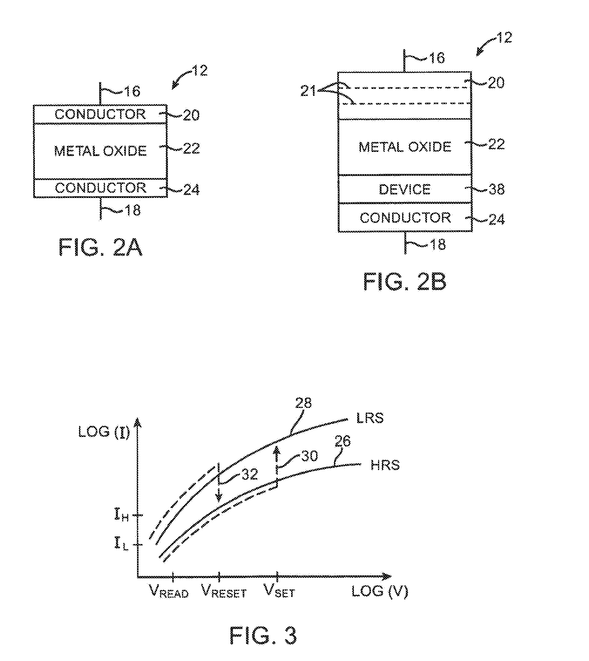
[0080]Samples of TaN produced by PVD with a nitrogen flow rate above about 50% generally had resistivities in the range of interest (0.1-10 Ω cm) as did the TaSiN sample. MN samples showed useful resistivities for nitrogen flow rates in the range 10-15%. The data suggest that the resistive layers comprising a sub-stoichiometric nitride or sub-stoichiometric oxynitride having the desired current limiting resistivity for any particular devic...


PUM

PropertyMeasurementUnit
resistivityaaaaaaaaaa
total pressureaaaaaaaaaa

Abstract

A nonvolatile memory element is disclosed comprising a first electrode, a near-stoichiometric metal oxide memory layer having bistable resistance, and a second electrode in contact with the near-stoichiometric metal oxide memory layer. At least one electrode is a resistive electrode comprising a sub-stoichiometric transition metal nitride or oxynitride, and has a resistivity between 0.1 and 10 Ω cm. The resistive electrode provides the functionality of an embedded current-limiting resistor and also serves as a source and sink of oxygen vacancies for setting and resetting the resistance state of the metal oxide layer. Novel fabrication methods for the second electrode are also disclosed.

Description

FIELD OF THE INVENTION[0001]One or more embodiments of the present invention relate to ReRAM devices and methods of making ReRAM devices, and more particularly to methods for forming electrodes having embedded resistor functionality.BACKGROUND[0002]Nonvolatile memory elements are used in systems in which persistent storage is required. For example, digital cameras use nonvolatile memory cards to store images and digital music players use nonvolatile memory to store audio data. Nonvolatile memory is also used to persistently store data in computer environments.[0003]Nonvolatile memory is often formed using electrically-erasable programmable read only memory (EEPROM) technology. This type of nonvolatile memory contains floating gate transistors that can be selectively programmed or erased by application of suitable voltages to their terminals.[0004]As fabrication techniques improve, it is becoming possible to fabricate nonvolatile memory elements with increasingly smaller dimensions. ...

Claims


Application Information

Patent Timeline
Patent Type & Authority Applications(United States)
IPC IPC(8): H01L45/00
CPCH01L45/1608H01L45/1625H01L45/08H01L45/1233H01L45/1266C23C14/345H01L45/146H01L45/16H01L27/2409H01L27/2463C23C14/0641H01L45/145C23C14/0042C23C14/083C23C14/225H10B63/20H10B63/80H10N70/24H10N70/801H10N70/8416H10N70/826H10N70/8833H10N70/883H10N70/011H10N70/021H10N70/023H10N70/026
Inventor PHAM, HIEUGOPAL, VIDYUTHASHIM, IMRANPRAMANIK, DIPANKARWANG, YUNYANG, HONG SHENG
Owner SANDISK TECH LLC
Why Eureka
Try Eureka