Micro-Pattern Forming Method, and Micro-Channel Transistor and Micro-Channel Light-Emitting Transistor Forming Method Using Same

a technology of micro-patterns and transistors, applied in the field of micro-pattern forming methods, can solve the problems of large amount of time and cost, complicated process, and expensive equipment using deep ultraviolet (uv) with expensive parts, and achieves high luminous efficiency, facilitates injection of holes and electrons, and high cost

Active Publication Date: 2013-08-08
POSTECH ACAD IND FOUND
View PDF3 Cites 38 Cited by
  • Summary
  • Abstract
  • Description
  • Claims
  • Application Information

AI Technical Summary

Benefits of technology

[0025]A method of forming a pattern having a microspacing according to an aspect of the present invention may accurately form a pattern having a microspacing over a large area and at a desired position by forming an organic wire or organic-inorganic hybrid wire mask pattern having a circular or elliptical cross section and forming a material layer thereon, and then removing the organic wire or organic-inorganic hybrid wire mask pattern. Since the formation of the organic wire or organic-inorganic hybrid wire mask pattern may be performed at room temperature and atmospheric pressure, the method may replace a typical high cost method of forming a micropattern, such as photolithography and E-beam lithography.
[0026]A method of

Problems solved by technology

Currently, since most of processes able to form nanoscale patterns on a substrate are based on vacuum technologies, these processes are complicated and expensive.
However, since a region on which a pattern may be formed is relatively localized, a relatively large amount of time and costs may be necessary in order to form a micropattern over a large area.
Thus, an expensive piece of equipment using a deep ultraviolet (UV) light source, such as a 248 nm KrF excimer laser or 193 nm ArF excimer laser, must be included in order to realize a nanoscale pattern.
Nevertheless, resolution may be limited to about 0.1 μm.
However, the foregoing process may have the following limitations; (1) Since nanowires are

Method used


Image

  • Micro-Pattern Forming Method, and Micro-Channel Transistor and Micro-Channel Light-Emitting Transistor Forming Method Using Same
  • Micro-Pattern Forming Method, and Micro-Channel Transistor and Micro-Channel Light-Emitting Transistor Forming Method Using Same
  • Micro-Pattern Forming Method, and Micro-Channel Transistor and Micro-Channel Light-Emitting Transistor Forming Method Using Same

Examples


example 1

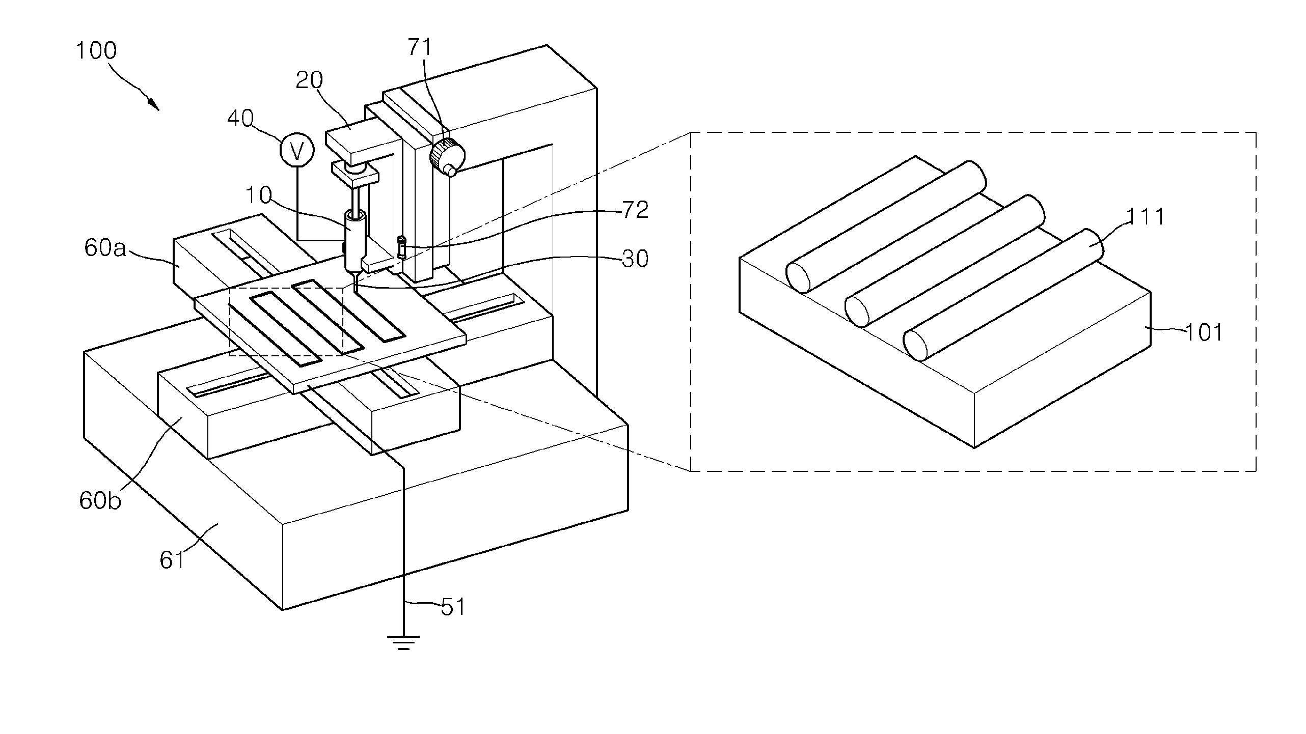
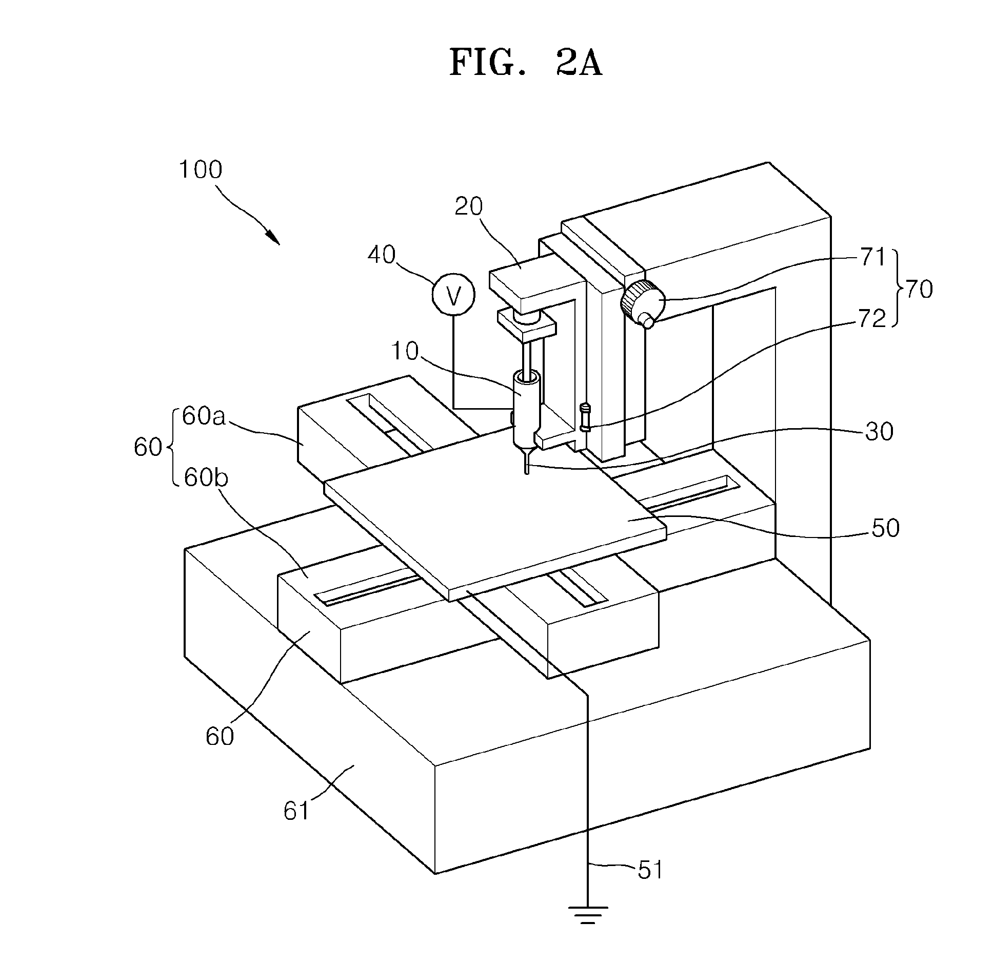
[0113]A pattern having a nanospacing formed of gold (Au) was prepared by using the method of forming a micropattern according to the embodiment of the present invention.

[0114]First, a nanowire mask pattern formed of a polymer material was formed on a substrate. In detail, poly(N-vinylcarbazole) (PVK) was first dissolved in styrene to prepare a PVK solution. The PVK solution was put in a syringe of an electric field aided robotic nozzle printer and the PVK solution was discharged from a nozzle while a voltage was applied to the nozzle. A PVK nanowire mask pattern was formed on the substrate on a collector moved by a robot stage.

[0115]At this time, a diameter of the nozzle used was 100 μm, a distance between the nozzle and the collector was 2.5 mm, an applied voltage was 4 kV, and a discharge speed of a solution was 500 nl / min. A movement spacing in a y-axis direction of the robot stage was 50 μm and a movement distance in an x-axis direction was 15 cm. A movement speed in the y-axis ...

example 2

[0120]A square pattern formed of gold having a nanospacing was prepared by using the method of forming a micropattern according to the embodiment of the present invention.

[0121]First, an orthogonal pattern composed of polymer nanowire mask patterns having a width of about 460 nm and a spacing of about 50 μm was prepared on a substrate. The polymer nanowire mask pattern was formed of PVK. In detail, as described in Example 1, PVK was first dissolved in styrene to prepare a PVK solution. The PVK solution was put in a syringe of an electric field aided robotic nozzle printer and the PVK solution was discharged from a nozzle while a voltage of 4 kV was applied to the nozzle. A robot stage was moved in an x-axis direction to form a nanowire mask pattern in the x-axis direction and the robot stage was moved in a y-axis direction to form a nanowire mask pattern in the y-axis direction, and thus a nanowire mask orthogonal pattern was formed.

[0122]At this time, a diameter of the nozzle used ...

example 3

[0126]A nanochannel thin film transistor was fabricated by using the method of forming a micropattern according to the embodiment of the present invention.

[0127]A titanium (Ti) gate electrode having a width of 600 μm and a thickness of 30 nm was formed on a silicon wafer. An aluminum oxide (Al2O3) gate dielectric layer having a thickness of 50 nm was formed on the gate electrode by atomic layer deposition. Gold electrodes having a spacing of 340 nm and a thickness of 70 nm were formed on the gate dielectric layer as source and drain electrodes.

[0128]First, a nanowire mask pattern having a diameter of about 350 nm and a spacing of about 5.5 mm was formed on a substrate having the Ti gate electrode and the Al2O3 gate dielectric layer formed thereon in order to form the gold electrodes having a nanospacing. The nanowire mask pattern was formed of PVK.

[0129]In detail, as described in Example 1, PVK was first dissolved in styrene to prepare a PVK solution. The PVK solution was put in a s...


PUM


Abstract

Provided is a method of forming a micropattern according to an aspect of the present invention. The method of forming a micropattern may include forming an organic wire or organic-inorganic hybrid wire mask pattern having a circular or elliptical cross section on a substrate, forming a material layer on an entire surface of the substrate having the organic wire or organic-inorganic hybrid wire mask pattern formed thereon, and removing the organic wire or organic-inorganic hybrid wire mask pattern from the substrate to allow only the material layer on a portion of the substrate having no organic wire or organic-inorganic hybrid wire mask pattern formed thereon to be remained.

Description

TECHNICAL FIELD[0001]The present invention relates to a method of forming a micropattern using an organic wire or an organic-inorganic hybrid wire, and more particularly, to a method of forming a micropattern using an organic wire or an organic-inorganic hybrid wire as a patterning mask and a method of forming an electronic device using the same.BACKGROUND ART[0002]Currently, since most of processes able to form nanoscale patterns on a substrate are based on vacuum technologies, these processes are complicated and expensive. For example, electron (E)-beam lithography may form micropatterns in vacuum. However, since a region on which a pattern may be formed is relatively localized, a relatively large amount of time and costs may be necessary in order to form a micropattern over a large area. Also, with respect to photolithography used in a semiconductor process, a size of a pattern is affected by a wavelength of a light source. Thus, an expensive piece of equipment using a deep ultra...

Claims


Application Information

Patent Timeline
IPC IPC(8): H01L51/00
CPCH01L51/0005B81C1/00031H01L51/0016H01L51/0023Y02E10/549H01L51/0545H01L51/102H01L51/428H01L51/5296H01L51/0541G03F7/164H10K71/221H10K71/621H10K10/464H10K10/82H10K10/466H10K30/65H10K50/30B82B3/0009H01L21/0274H01L29/78H10K71/135
Inventor MIN, SUNG YONGKIM, TAE SIKLEE, TAE-WOO
Owner POSTECH ACAD IND FOUND
Why Eureka
Try Eureka