Heat treatment apparatus for heating substrate by irradiation with flashes of light, and heat treatment method

a technology of heat treatment apparatus and electronic substrate, which is applied in lighting and heating apparatus, muffle furnaces, furnaces, etc., can solve the problems of reducing throughput, affecting the formation of devices, and requiring a long time for preheating, so as to prevent the cracking of the substrate and reduce the degree of degree of

Active Publication Date: 2013-08-08
DAINIPPON SCREEN MTG CO LTD
View PDF31 Cites 73 Cited by
  • Summary
  • Abstract
  • Description
  • Claims
  • Application Information

AI Technical Summary

Benefits of technology

[0026]Therefore, an object of the present invention is to reduce the degree to which the light absorption rate in the surface of the substrate depends on a pattern thereon during irradiation with flashes of light.
[0027]Another object of the present invention is to prevent cracking of the substrate during irradiation with flashes of light.
[0028]Still another object of the present invention is to complete all heat treatments in a short time.

Problems solved by technology

When a length of annealing time in this annealing process is equal to or longer than about several seconds, the implanted impurities are deeply diffused due to heat, and consequently a junction depth is excessively greater than required, which may hinder successful formation of a device.
Even though the flash heating is performed only for several milliseconds, the preheating requiring a long time not only lowers the throughput but also raises the temperature of component parts included a chamber that receives the semiconductor wafer therein.
As a result, a problem arises that the rate of temperature drop of the semiconductor wafer after the flash heating is lowered.
Such damage is often formed in a step prior to the flash lamp annealing.
This causes a problem that wafer cracking originating at the damage of the back surface occurs.
Therefore, the absorption rate in a plane of the surface is not uniform.
That is, since the light absorption rate in the surface of the semiconductor wafer depends on the pattern, a problem arises that the temperature distribution in a wafer plane is non-uniform during irradiation with flashes of light.

Method used


Image

  • Heat treatment apparatus for heating substrate by irradiation with flashes of light, and heat treatment method
  • Heat treatment apparatus for heating substrate by irradiation with flashes of light, and heat treatment method
  • Heat treatment apparatus for heating substrate by irradiation with flashes of light, and heat treatment method

Examples


first preferred embodiment

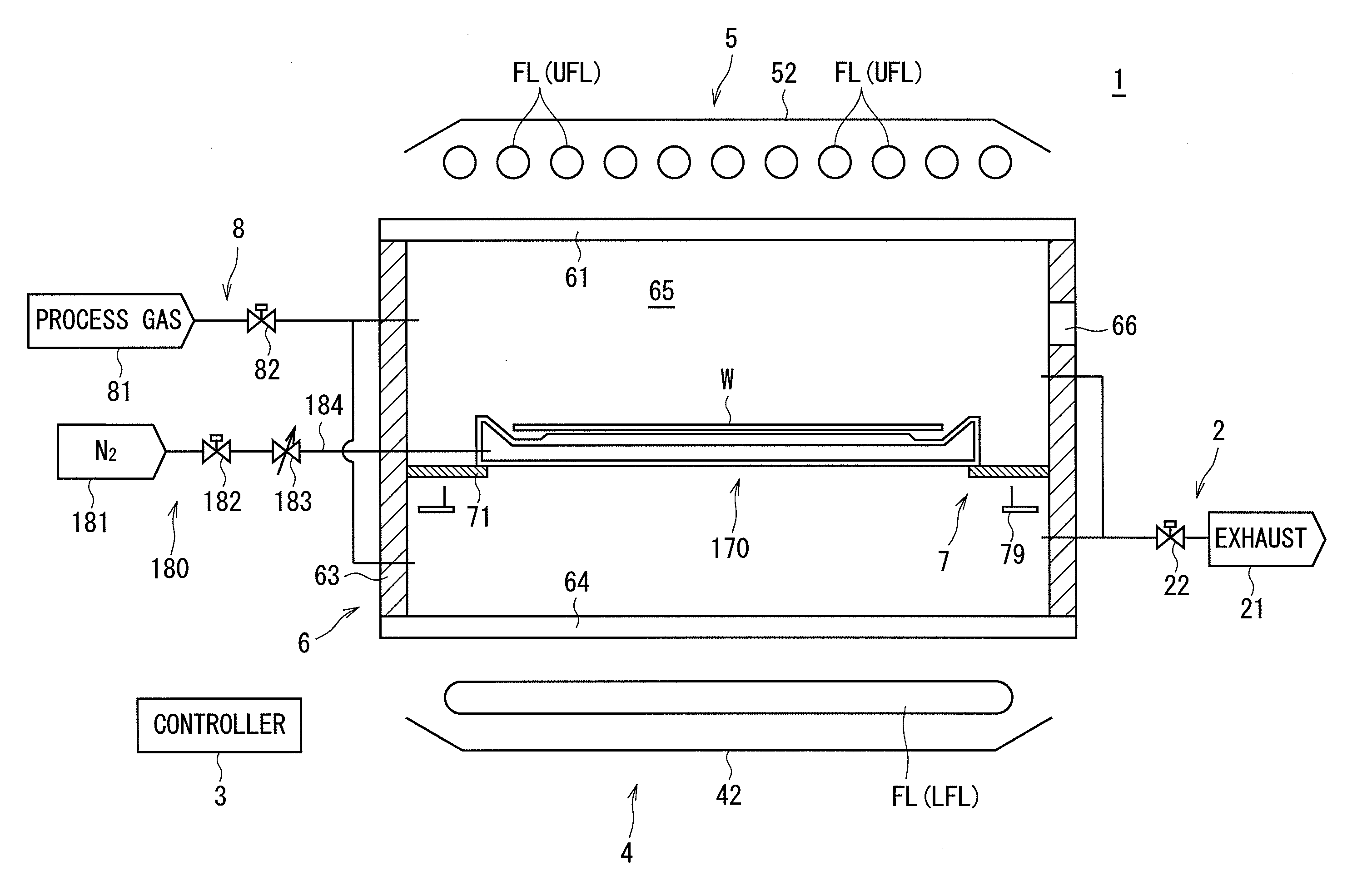
[0074]FIG. 1 is a diagram showing a configuration of principal parts of a heat treatment apparatus 1 according to the present invention. The heat treatment apparatus 1 is a flash lamp annealer that performs a heat treatment on a substantially circular semiconductor wafer W serving as a substrate by irradiating the semiconductor wafer W with flashes of light. In FIG. 1 and subsequent Figures, the dimensions of components and the number of components are shown in exaggeration or in simplified form, as appropriate, for the sake of easier understanding.

[0075]The heat treatment apparatus 1 principally includes a chamber 6, a holder 7, a transfer part 79, an upper heating part 5, a lower heating part 4, a gas supply part 8, and an exhaust part 2. The chamber 6 has a substantially cylindrical shape, and receives the semiconductor wafer W therein. The holder 7 holds the semiconductor wafer W within the chamber 6. The transfer part 79 exchanges the semiconductor wafer W with the holder 7. Th...

second preferred embodiment

[0138]Next, a second preferred embodiment of the present invention will be described. A configuration of a heat treatment apparatus according to the second preferred embodiment is exactly the same as that of the first preferred embodiment. The second preferred embodiment is different from the first preferred embodiment in terms of a timing when the flash lamp FL emits light.

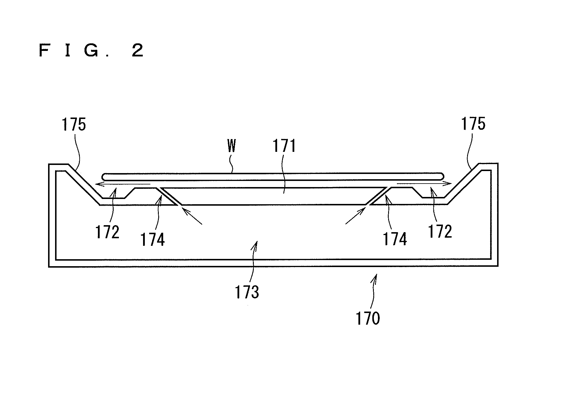
[0139]In the second preferred embodiment, until the irradiation with flashes of light (that is, until step S13 of FIG. 5), the same process steps as those of the first preferred embodiment are performed on the semiconductor wafer W. More specifically, the semiconductor wafer W serving as the processing object is transported into the chamber 6 and adsorptively held in a non-contact fashion by the Bernoulli chuck 170. The gas supply part 8 and the exhaust part 2 create a nitrogen atmosphere in the heat treatment space 65 of the chamber 6.

[0140]After the semiconductor wafer W is held in a non-contact fashion by the ...

third preferred embodiment

[0149]Next, a third preferred embodiment of the present invention will be described. FIG. 11 is a diagram showing a configuration of principal parts of a heat treatment apparatus 1a according to the third preferred embodiment. In FIG. 11, the same elements as those of the first preferred embodiment shown in FIG. 1 are denoted by the same corresponding reference numerals. The third preferred embodiment is different from the first preferred embodiment, in that only the upper heating part 5 provided above the chamber 6 serves as a heat source.

[0150]In the third preferred embodiment, the lower opening of the chamber 6 is closed with a disk-shaped member made of the same metal material as that of the chamber side portion 63. In the upper opening of the chamber 6, the upper chamber window 61 similar to that of the first preferred embodiment is mounted.

[0151]The upper heating part 5 is configured in the same manner as in the first preferred embodiment. To be specific, the upper heating par...


PUM


Abstract

A first flash heating is performed in which a lower flash lamp irradiates a back surface of a semiconductor wafer with flashes of light, so that heat conduction from the back surface to a surface of the semiconductor wafer raises the temperature of the surface from the room temperature to an intermediate temperature. Then, a second flash heating is performed in which an upper flash lamp irradiates the surface of the semiconductor wafer with flashes of light, to raise the temperature of the surface of the semiconductor wafer from the intermediate temperature to a target temperature. Since only the irradiation with flashes of light emitted from the lower flash lamp and the upper flash lamp is used to cause the semiconductor wafer having the room temperature to reach the target temperature, all heat treatments can be completed in an extremely short time of one second or less.

Description

BACKGROUND OF THE INVENTION[0001]1. Field of the Invention[0002]The present invention relates to a heat treatment apparatus and a heat treatment method for heating a thin plate-like precision electronic substrate (hereinafter, simply referred to as “substrate”), such as a semiconductor wafer and a glass substrate for a liquid crystal display device, by irradiating the substrate with flashes of light.[0003]2. Description of the Background Art[0004]In a process for manufacturing a semiconductor device, impurity doping is an essential step for forming a pn junction in a semiconductor wafer. At present, it is common practice to implement the impurity doping through an ion implantation process and a subsequent annealing process. The ion implantation process is a technique of ionizing impurity elements such as boron (B), arsenic (As), and phosphorus (P) and causing ions of the impurity elements to collide against the semiconductor wafer with a high acceleration voltage, to thereby physica...

Claims


Application Information

Patent Timeline
Patent Type & Authority Applications(United States)
IPC IPC(8): H01L21/26F27D11/12
CPCH01L21/26F27D11/12H01L21/6838F27B17/0025F27D5/0037F27B17/0016F27B5/14F27B5/18
Inventor YOKOUCHI, KENICHI
Owner DAINIPPON SCREEN MTG CO LTD
Why Eureka
Try Eureka