Architecture and method for remote memory system diagnostic and optimization

a memory system and architecture technology, applied in the field of smart memory architecture, can solve the problems of insufficient availability of memory repair to the memory's end user, not all memory cells on the memory chip functioning properly, and conventional approaches to detecting and solving memory defects are inadequate, so as to facilitate real-time diagnosis and repair

Inactive Publication Date: 2013-08-15
SAMSUNG ELECTRONICS CO LTD
View PDF19 Cites 26 Cited by
  • Summary
  • Abstract
  • Description
  • Claims
  • Application Information

AI Technical Summary

Benefits of technology

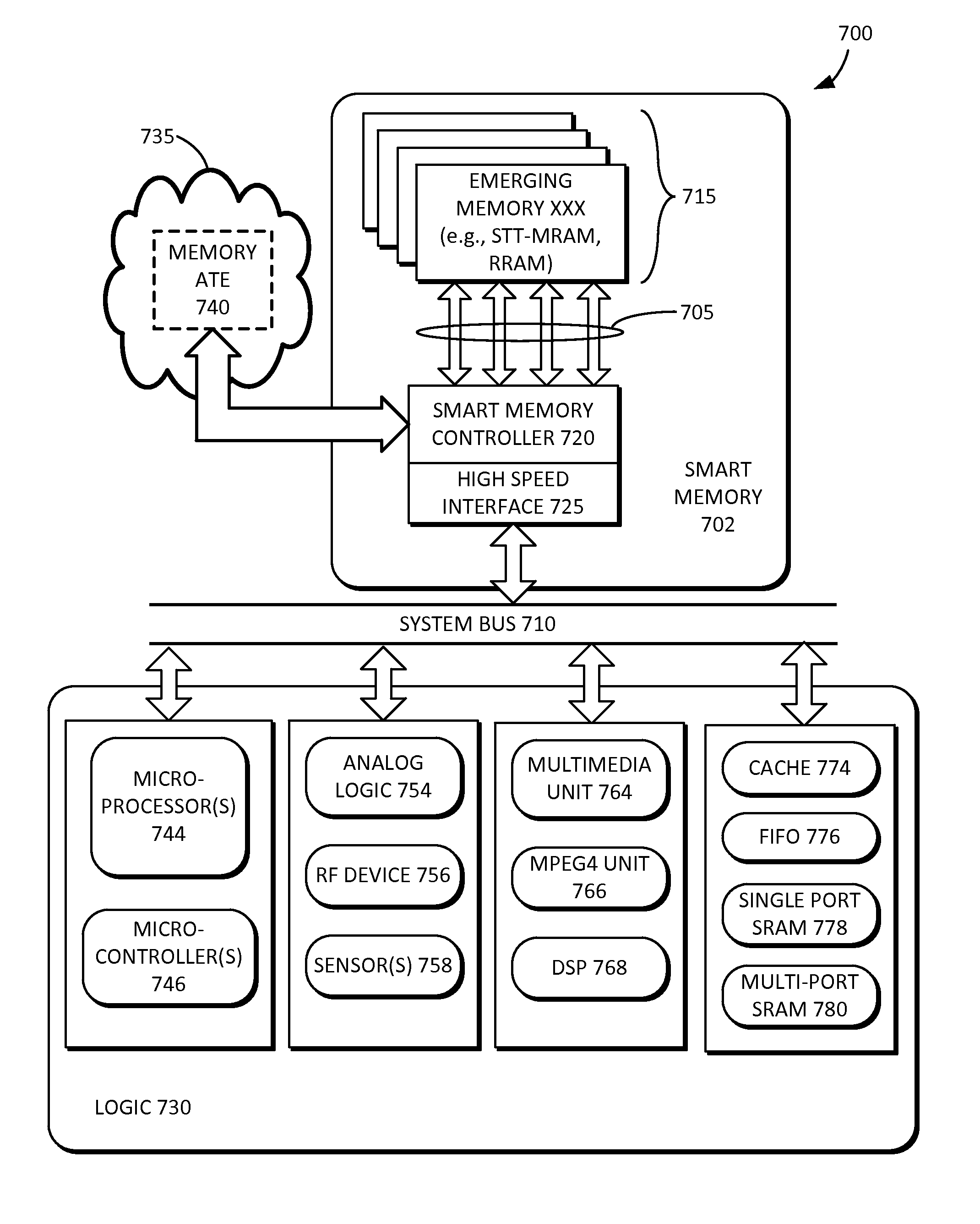
[0026]According to features and principles of the present inventive concepts, a smart memory system can be operatively coupled to a remote system enhancement and recovery entity via a secure cloud connection. The smart memory system, when implemented in an internet-connectable device, can be provided with tools that permit the memory system to be accessed and optimized anytime, and anywhere the device has cloud access. For instance, remote testing equipment can be accessed and utilized by the device based on user-initiated or automatically generated test instructions. The smart memory system can further facilitate real-time diagnosis and repair by a remotely-located application engineer or other entity.
[0029]Certain of the inventive features may be best achieved by implementing them in a System-in-Package (SiP) or System-on-Chip (SoC). Such implementations need good connectivity between a memory array and memory processor chips. This may be accomplished, for instance, using True Silicon Via (TSV) or other SiP technology. Using low latency and high throughput SiP interconnects can provide improved system performance. The cost disadvantages of such a system may be minimized as SiP interconnect technology costs continue to decrease.
[0030]The inventive principles can also enable reduced power consumption by reducing I / O loading using SiP solutions, by providing clock-less memory operation, and / or by shutting down unused memory sections. Voltage control, temperature compensation, and asynchronous timing circuitry can also help reduce power consumption and provide more efficient operation.
[0031]Other principles allow the device processor to offload repetitive computations or other tasks to the smart memory system. For instance, an ARM, MIPs, or other desired proprietary processor combination can be provided in the memory controller or other area of the smart memory system to perform various processing tasks to free up device resources.
[0032]Memory monitoring, repair, correction, and re-assignment can also be performed by the smart memory controller and / or remotely according to principles of the present inventive concept. ECC, anti-fuse repair, error masking, read-compare-write, weak bit replacement, and other error correction technologies can be implemented in the smart memory system to enhance data stability and reduce error rates.

Problems solved by technology

Unfortunately, with STT-RAM or any other type of memory chip, manufacturing or other defects may result in not all memory cells on a memory chip functioning properly.
Memory repair is not made available to the memory's end-user.
Due to the relatively high error rates and probabilistic tendencies of memories such as PCRAM, MRAM, and RRAM devices, the conventional approaches to detecting and solving memory defects are inadequate.
Once in the field, it is difficult or impossible to fully diagnose and apply repair solutions to the memory systems.

Method used


Image

  • Architecture and method for remote memory system diagnostic and optimization
  • Architecture and method for remote memory system diagnostic and optimization
  • Architecture and method for remote memory system diagnostic and optimization

Examples


Embodiment Construction

[0054]Reference will now be made in detail to embodiments of the inventive concept, examples of which are illustrated in the accompanying drawings. In the following detailed description, numerous specific details are set forth to enable a thorough understanding of the inventive concept. It should be understood, however, that persons having ordinary skill in the art may practice the inventive concept without these specific details. In other instances, well-known methods, procedures, components, circuits, and networks have not been described in detail so as not to unnecessarily obscure aspects of the embodiments.

[0055]It will be understood that, although the terms first, second, etc. may be used herein to describe various elements, these elements should not be limited by these terms. These terms are only used to distinguish one element from another. For example, a first circuit could be termed a second circuit, and, similarly, a second circuit could be termed a first circuit, without ...


PUM


Abstract

A smart memory system preferably includes a memory including one or more memory chips and a smart memory controller. The smart memory controller includes a transmitter communicatively coupled to the cloud. The transmitter securely transmits a product identification (ID) associated with the memory to the cloud. A cloud-based data center receives and stores the product ID and related information associated with the memory. A smart memory tester receives a product specific test program from the cloud-based data center. The smart memory tester may remotely test the memory via the cloud in accordance with the product specific test program. The information stored in the cloud-based data center can be accessed anywhere in the world by authorized personnel. Repair solutions can be remotely determined based on the test results and the diagnostic information. The repair solutions are transmitted to the smart memory controller, which repairs the memory.

Description

CROSS-REFERENCES TO RELATED APPLICATIONS[0001]This application claims the benefit of commonly assigned provisional application Ser. No. 61 / 597,773, filed Feb. 11, 2012, entitled “A METHOD AND SYSTEM FOR PROVIDING A SMART MEMORY ARCHITECTURE,” the contents of which is incorporated herein by reference in its entirety.BACKGROUND[0002]The present inventive concepts relate to a smart memory architecture, and more particularly to an architecture and method for remotely diagnosing and optimizing memory systems.[0003]The present inventive concepts relate to memory systems for storing and retrieving information from memory integrated circuits, including static random access memory (SRAM), dynamic random access memory (DRAM), Flash memory, phase-change random access memory (PCRAM), spin-transfer torque random access memory (STT-RAM), magnetic random access memory (MRAM), resistive random access memory (RRAM), and future memory devices. Inventive aspects described herein are particularly well-...

Claims


Application Information

Patent Timeline
Patent Type & Authority Applications(United States)
IPC IPC(8): G06F15/167
CPCG06F15/167G06F11/0751G06F11/0793G06F12/00G06F3/0601G06F21/00G11C13/0002G06F11/1076G06F11/1008G11C11/16G11C11/1677G11C11/1695G11C29/00
Inventor ONG, ADRIAN E.
Owner SAMSUNG ELECTRONICS CO LTD
Why Eureka
Try Eureka