Methods and Apparatus For Patterning Photovoltaic Devices and Materials For Use With Such Devices

a photovoltaic device and patterning technology, applied in the direction of manufacturing tools, nuclear engineering, therapy, etc., can solve the problems of reducing the effective area, generating unacceptable resistive losses in relatively thin conductive films, and reducing the current flowing in each device, so as to improve the scribing

Active Publication Date: 2013-09-19
NKT PHOTONICS
View PDF3 Cites 12 Cited by
  • Summary
  • Abstract
  • Description
  • Claims
  • Application Information

AI Technical Summary

Benefits of technology

[0013]The incorporation of a harmonic module in the assembly of the present invention produces a second laser wavelength with a spectral bandwidth which has improved spectral matching to the beam shaping elements, compared with the first laser wavelength. As a result the assembly provides for a more uniform intensity profile across the beam, compared with that which would be obtained with the first laser wavelength, and thus an improved scribe in photovoltaic device materials, by minimizing interlayer mixing and heating, in addition to improved side wall sharpness of the scribe.
[0016]The second spectral bandwidth, in comparison to the first spectral bandwidth, is arranged to more closely correspond with the spectral bandwidth of the at least one beam shaping element (i.e., less of the second spectral bandwidth, if any, is in excess of a bandwidth of the at least one beam shaping element, as compared to the first spectral bandwidth, which typically exceeds the spectral bandwidth of the at least one beam shaping element). A pulsed laser beam bandwidth which is less than or equal to the bandwidth of the at least one beam shaping element can be acceptable, and still “corresponds” to the spectral bandwidth of the at least one beam shaping element, as that term is used herein). Accordingly, laser beam shaping can be improved by shaping a pulsed laser beam having the second spectral bandwidth, in comparison with the shaping of a pulsed laser beam having the first spectral bandwidth.
[0017]As the skilled worker will understand from the present disclosure, the proper shaping of the laser beam is related to the correspondence between the second spectral bandwidth and the spectral bandwidth of the optical element of the beam shaping apparatus. If the bandwidths do not substantially correspond then the shaped laser beam will not have the desired substantially rectangular intensity profile. Shaping is broadly desirable because the sharp or steep sidewalls can improve scribing as compared to the use of a Gaussian beam having Gaussian sidewalls.
[0058]delivering a pulsed laser beam to the selected target layers of layers to remove the selected target material; wherein the laser beam comprises a wavelength in the range of 500-555 nm, a pulse width in range of 0.1 ps to 100 ps, a pulse repetition rate in the range of 100 kHz to 500 kHz, and a fluence in the range of 0.1 J / cm2 to 10 J / cm2; and wherein the laser beam can substantially remove the target material so as to expose at least part of the surface of the non target region and effect such removal without appreciably detrimentally affecting the exposed surface as regards the functionality of the photovoltaic structure.

Problems solved by technology

In situations where the operating voltage is 0.6V, this would relate to an operating current of several hundred amperes, and thus generate unacceptable resistive losses in the relatively thin conductive films.
As a result, it is common to divide or scribe the panel into individual devices having a width of only a few hundred microns, to reduce the effective area and thus reduce the current flowing in each device.
Unfortunately, as those skilled in the art will recognize, nanosecond laser scribing of TCO materials employed in a-Si photovoltaic devices typically suffers from substantial heating and related micro-cracking which can compromise device performance, leading to premature device failure and consequently a higher unit price per device.
The reduced pulse duration is found to reduce the heating of the TCO; however, such lasers typically produce a very narrow pulsewidth range due to the limitations of the mode-locking methods employed to generate the picosecond seed pulses produced by the oscillators in these devices.
Picosecond mode-locked diode pumped solid state lasers typically contain many free-space coupled optics, which are difficult to maintain in proper alignment.
Furthermore, such laser systems are known to be relatively expensive in comparison to nanosecond diode pumped solid state lasers and their cost remains a barrier to wide industrial application.
If the bandwidths do not substantially correspond then the shaped laser beam will not have the desired substantially rectangular intensity profile.

Method used


Image

  • Methods and Apparatus For Patterning Photovoltaic Devices and Materials For Use With Such Devices
  • Methods and Apparatus For Patterning Photovoltaic Devices and Materials For Use With Such Devices
  • Methods and Apparatus For Patterning Photovoltaic Devices and Materials For Use With Such Devices

Examples


Embodiment Construction

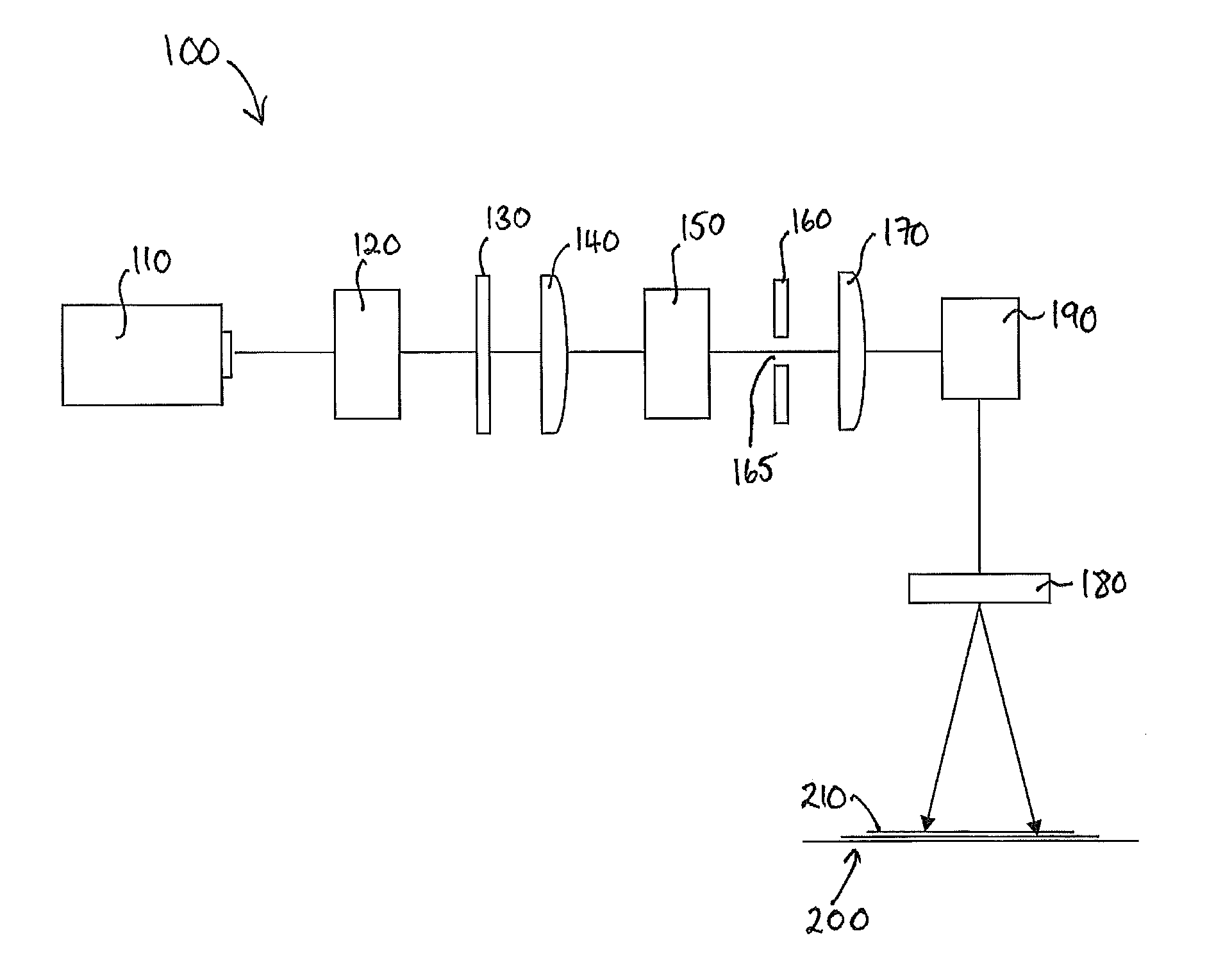
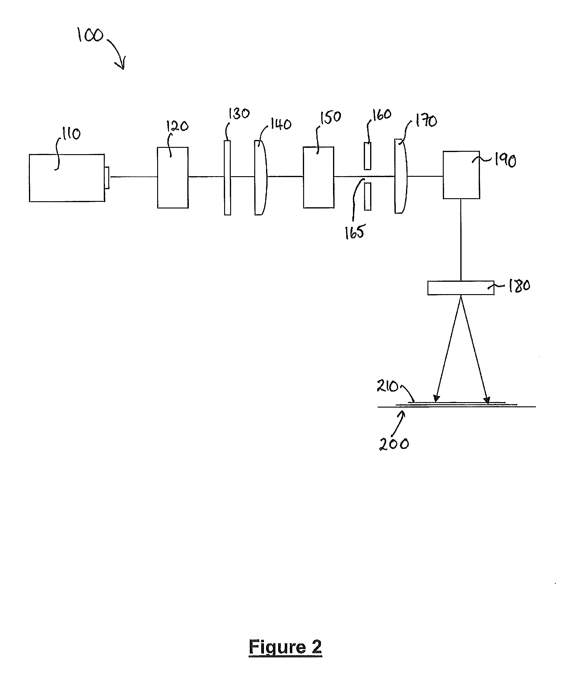
[0093]Referring to FIG. 2 of the drawings, there is illustrated a laser beam shaping assembly 100 according to a first embodiment of the present invention for shaping a picosecond laser beam which is used to pattern a photovoltaic devices 200 (e.g., scribe thin film photovoltaic devices), including patterning regions comprising amorphous silicon (a-Si), silicon nitride, silicon oxide or cadmium telluride. The assembly 100 comprises an ultrafast fibre laser, which is arranged to generate laser pulses with a pulse repetition frequency in the range of 10 kHz to 100 MHz and more preferably 100 kHz to 500 kHz. The laser may comprise a diode-pumped ultrafast master oscillator fibre power amplifier (UFMOFPA) 110, or alternatively a diode-pumped flexible ultrafast master oscillator fibre power amplifier, both of which are arranged to generate a fundamental laser wavelength in the range 0.2 μm to 1.6 μm and most preferably substantially 1 μm, and picoseconds laser pulses with a pulse within ...


PUM

PropertyMeasurementUnit
wavelengthaaaaaaaaaa
laser wavelengthaaaaaaaaaa

Abstract

A picosecond laser beam shaping assembly is disclosed for shaping a picosecond laser beam for use in patterning (e.g., scribing) semiconductor devices. The assembly comprises a pulsed fibre laser source of picosecond laser pulses, a harmonic conversion element for converting laser pulses at a first laser wavelength having a first spectral bandwidth to laser pulses at a second laser wavelength having a second spectral bandwidth, and a beam shaping apparatus for shaping the laser beam at the second laser wavelength, the beam shaping apparatus having a spectral bandwidth that substantially corresponds to the second spectral bandwidth so as to produce a laser beam having a substantially rectangular cross-sectional profile.

Description

FIELD OF THE INVENTION[0001]The present invention relates to a picosecond laser beam shaping assembly and particularly, but not exclusively, to a picosecond laser beam shaping assembly for shaping a picosecond laser beam which is used in patterning (e.g., scribing) photovoltaic devices. The present invention also relates to a method of spatially shaping a picosecond laser beam which is output from a fibre laser, for use in the patterning of photovoltaic devices.BACKGROUND OF THE DISCLOSURE[0002]Thin film photovoltaic solar panels are generally used to harvest solar radiation to produce electricity and typically comprise a plurality of thin films of material deposited on a sheet of glass. The panels may comprise an effective panel area of several square metres, in which case, a panel with a 15% efficiency which receives 1000 W / m2 will generate several hundred Watts of electrical power. In situations where the operating voltage is 0.6V, this would relate to an operating current of sev...

Claims


Application Information

Patent Timeline
Patent Type & Authority Applications(United States)
IPC IPC(8): H01L31/18H01L21/78
CPCB23K26/0635B23K26/0732B23K26/367B23K26/409H01L21/268H01L31/073H01L31/0463Y02E10/543H01L21/78H01L31/18H01L31/0236H01L31/046H01L31/0749B23K26/0624B23K26/364B23K26/40B23K2103/172Y02E10/541
Inventor BAIRD, BRIAN W.GERKE, TIMOTHY D.
Owner NKT PHOTONICS
Why Eureka
Try Eureka