

Polishing pad and method for producing same
a technology of polishing pad and surface, which is applied in the field of polishing pad, can solve the problems of uneven surface area of polishing pad, decreased polishing speed, and scratching (flaws) on the surface, and achieve the effect of improving the dressing property
- Summary
- Abstract
- Description
- Claims
- Application Information
AI Technical Summary
Benefits of technology
Problems solved by technology
Method used
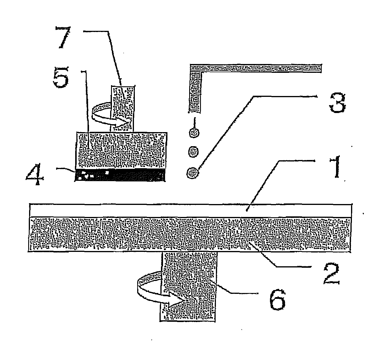
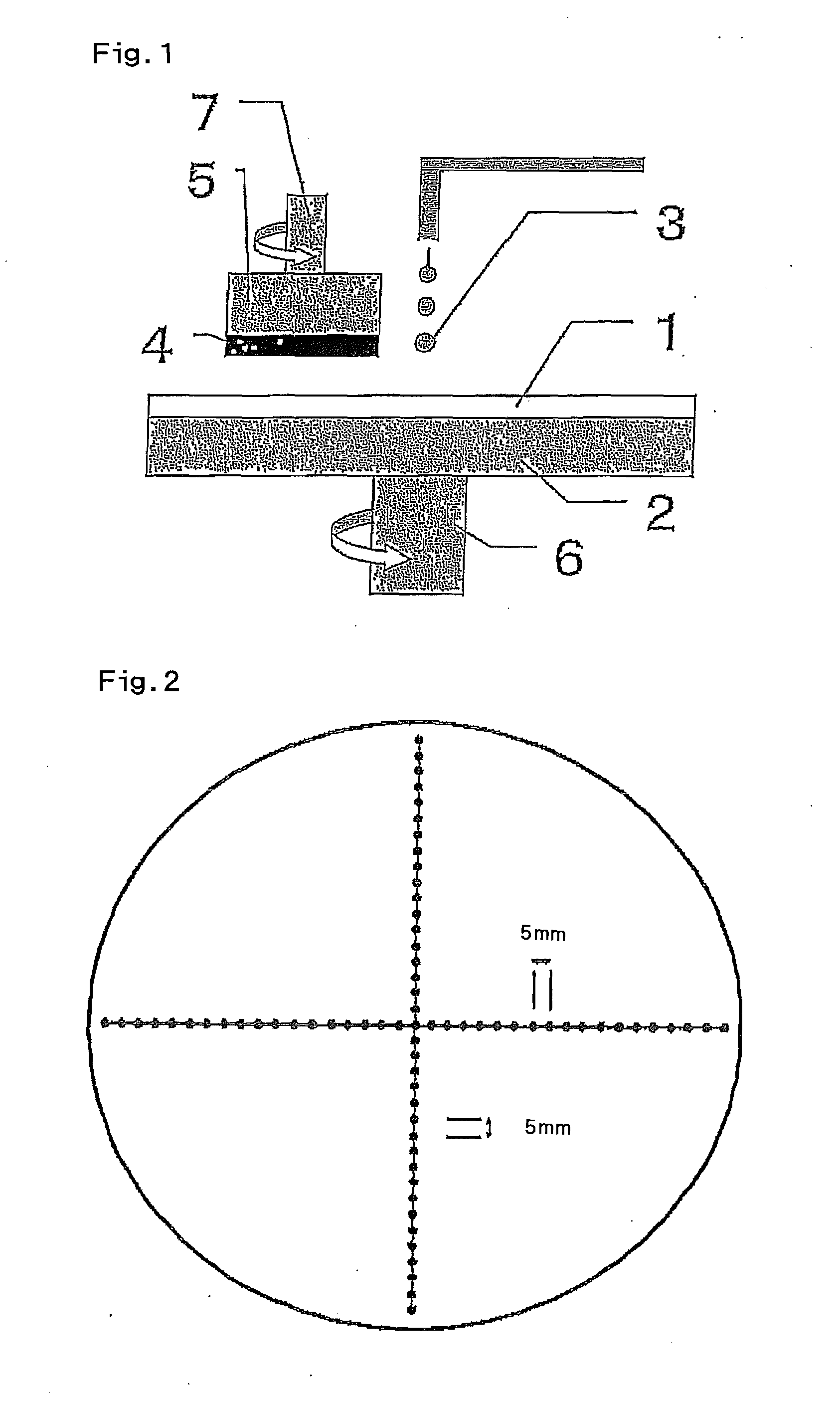
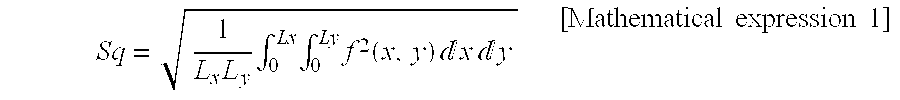
Image

Examples
example 1
[0073]To a vessel were added 1229 parts by weight of toluene diisocyanate (a mixture of toluene 2,4-diisocyanate / toluene 2,6-diisocyanate=80 / 20), 272 parts by weight of 4,4′-dicyclohexylmethane diisocyanate, 1901 parts by weight of polytetramethylene ether glycol with a number average molecular weight of 1018, and 198 parts by weight of diethylene glycol, and the mixture was allowed to react at 70° C. for 4 hours to obtain an isocyanate-terminated prepolymer. One hundred parts by weight of the prepolymer and 10 parts by weight of a polymerized 1,6-hexamethylene diisocyanate (Sumijule N-3300 (isocyanurate type) manufactured by Sumika Bayer Urethane Co., Ltd.) were mixed in a planetary mixing and defoaming apparatus and defoamed. After that, 32.9 parts by weight of 4,4′-methylenebis(o-chloroaniline) which had been melted at 120° C. was added to the mixture and mixed in the planetary mixing and defoaming apparatus, and then defoamed to prepare a polyurethane raw material composition. T...
example 2
[0075]A polishing pad was prepared in the same manner as in Example 1, except that in Example 1, the addition amount of Sumijule N-3300 was changed to 5 parts by weight from 10 parts by weight and the addition amount of 4,4′-methylenebis(o-chloroaniline) was changed to 29.7 parts by weight from 32.9 parts by weight.
example 3
[0076]A polishing pad was prepared in the same manner as in Example 1, except that in Example 1, 10 parts by weight of a polymerized 1,6-hexamethylene diisocyanate (Sumijule N-3200, biuret type, manufactured by Sumika Bayer Urethane Co., Ltd.) as an isocyanate-modified body was used in place of Sumijule N-3300, and the addition amount of 4,4′-methylenebis(o-chloroaniline) was changed to 33.2 parts by weight from 32.9 parts by weight.
PUM
| Property | Measurement | Unit |
|---|---|---|
| thickness | aaaaa | aaaaa |
| humidity | aaaaa | aaaaa |
| humidity | aaaaa | aaaaa |
Abstract
Description
Claims
Application Information