Eureka AIR delivers breakthrough ideas for toughest innovation challenges, trusted by R&D personnel around the world.

Substrates with conductive coatings

a technology of conductive coatings and substrates, applied in the field of substrates with conductive coatings, can solve the problems of increasing the cost of this procedure, difficult and expensive uniform film, complicated procedure, etc., and achieve excellent electronic, thermal and mechanical properties

Inactive Publication Date: 2013-10-03
XEROX CORP
View PDF2 Cites 8 Cited by
  • Summary
  • Abstract
  • Description
  • Claims
  • Application Information

AI Technical Summary

Benefits of technology

The patent describes how to make a layered material (such as graphene or nanoplate graphite) coat a substrate without using solvents. This results in electronic devices that have good electronics, heat, and mechanical properties. The patent also describes how to make large area uniform coatings and devices using this substrate.

Problems solved by technology

Unfortunately, the deposition of some layered materials, such as graphene and nanoplate graphite, into a large area, uniform film is difficult and expensive because these materials cannot be dispersed at a high concentration in common solvents for conventional coating methods.
However, this procedure is complicated and uses large amounts of solvents, which can be expensive during manufacturing.
Some solvents are also regulated materials, and compliance with disposal regulations further increases the costs of this procedure.

Method used

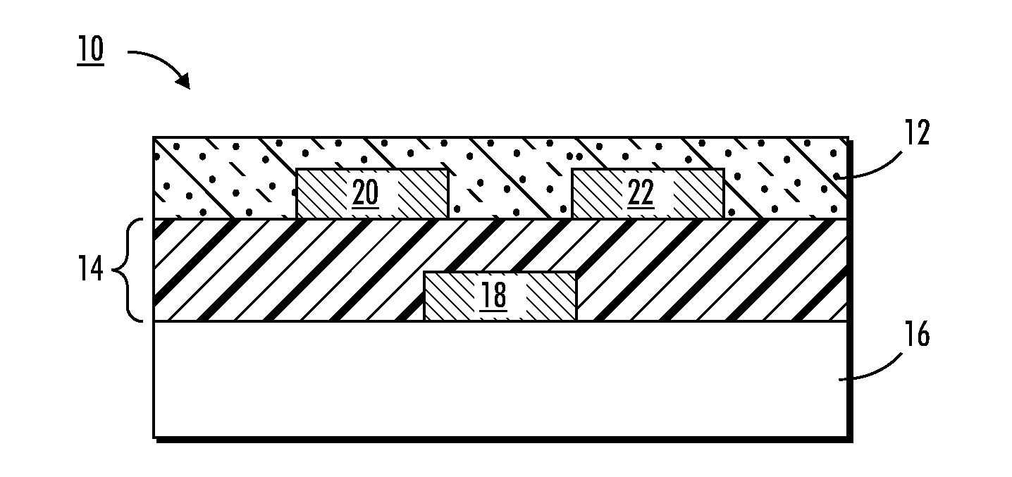
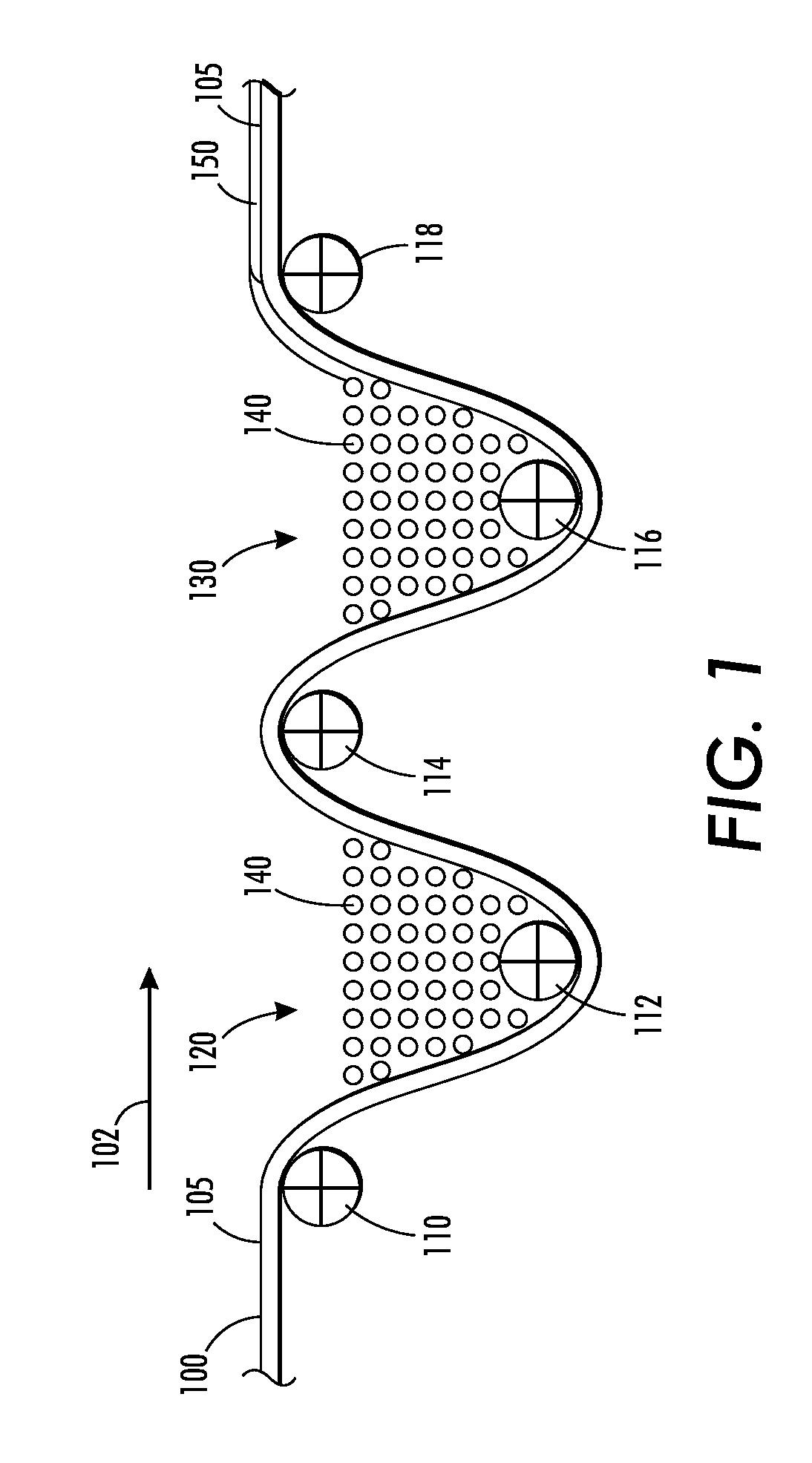
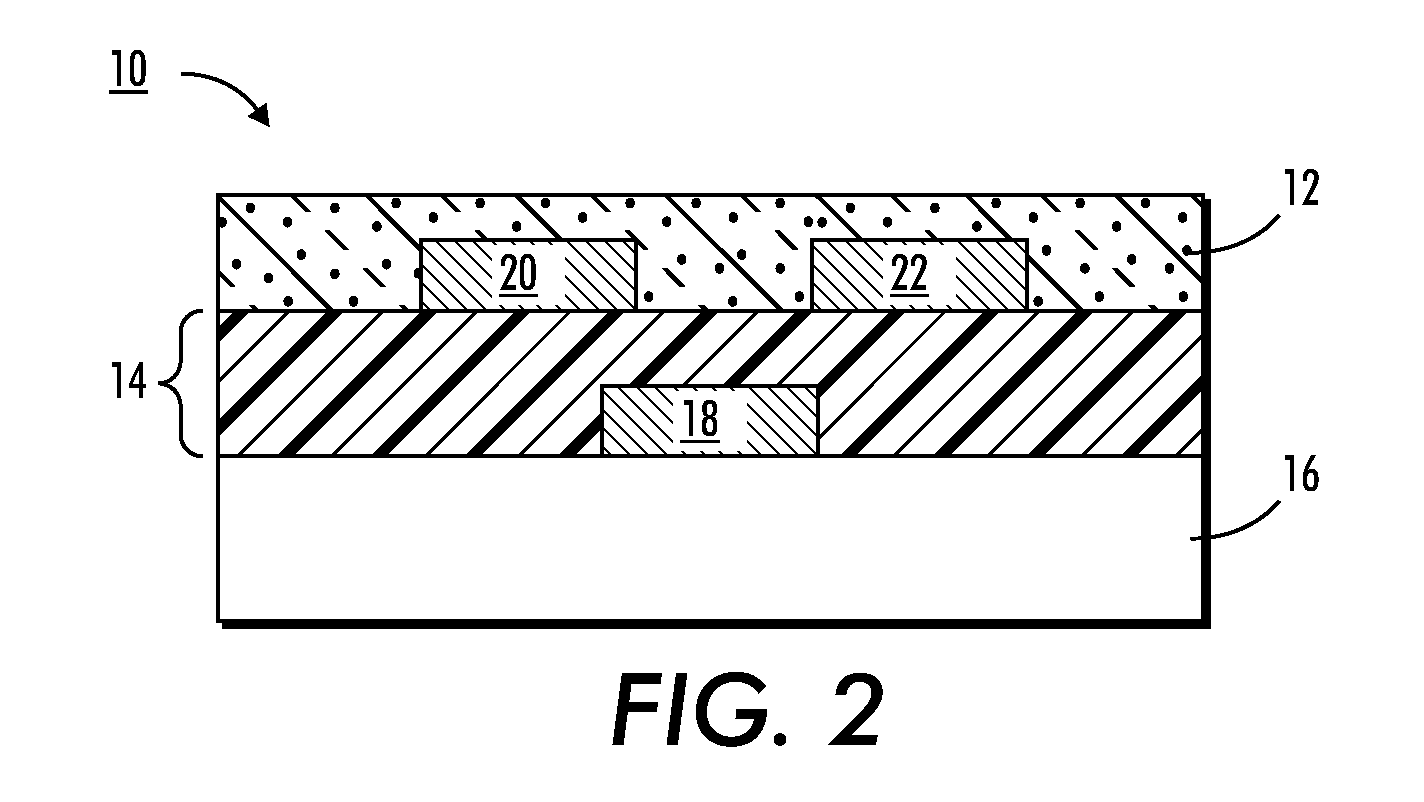

Image

  • Substrates with conductive coatings
  • Substrates with conductive coatings
  • Substrates with conductive coatings

Examples


example 1

[0082]0.1 grams of graphite flakes (from Sigma-Aldrich) were mixed with 4.0 grams of glass beads. The glass beads had a diameter of about 1 millimeter. The mixture was shaken for 30 minutes. After the mixture was shaken, the surface of the beads became black, indicating that the beads were coated with graphene and nanoplate graphite.

[0083]One side of a polyethylene terephthalate (PET) substrate was covered with Scotch tape. The substrate was placed in contact with the glass bead mixture and shaken for 30 minutes. After shaking, the uncovered surface of the PET substrate and the Scotch tape were covered with graphene and nanoplate graphite. Each surface of the substrate became highly conductive. The resistance of the Scotch tape side was measured using a two-probe ohm meter at 150 ohms for a length of about 5 cm and the resistance of the PET film was measured at 1,500 ohms for a length of about 5 cm. As a point of reference, a similar resistance measurement for indium-tin oxide (ITO)...

example 2

[0089]0.2 grams of natural graphite was placed in a 60 milliliter bottle. Metal shots (from Hoover Precision Product) having a diameter of one-eighth of an inch were added to fill half of the volume of the bottle. The mixture was milled on a milling machine for 3 hours. The metal shots became black, indicating that the surfaces of the shots were coated with graphene and nanoplate graphite.

[0090]Approximately 20 of the coated metal shots were removed and transferred to a second bottle. Fresh, i.e. clean, metal shots were added to the second bottle until half the volume of the bottle was filled. The mixture of the second bottle was milled for 30 minutes. All of the metal shots became black.

[0091]A PET substrate was inserted into the second bottle which was then shaken for 10 minutes, resulting in a smooth, shiny graphite / nanoplate graphene coating on both sides of the PET substrate. The surface conductivity of the coating was measured to be similar to the conductivity measured in Exam...

example 3

[0093]0.2 grams of graphite flakes (from Sigma-Aldrich) were mixed with 40.0 grams of glass beads. The glass beads had a diameter of about 1 millimeter. The mixture was shaken for 5 minutes using a Resodyn™ Acoustic Mixer (LabRAM Mixer). The surface of the beads became black immediately, indicating that the beads were coated with graphene and nanoplate graphite. A piece of PET substrate (2 centimeters by 5 centimeters) was immersed in the coated beads, and the container with the PET was allowed to shake in the LabRAM Mixer for 5 minutes, resulting in a smooth, shiny graphite / nanoplate graphene coating on both sides of the PET substrate.


PUM

PropertyMeasurementUnit
Thicknessaaaaaaaaaa
Thicknessaaaaaaaaaa
Electrical conductivityaaaaaaaaaa

Abstract

Disclosed herein are substrates which have been dry coated with a layered material. Generally, a layered material precursor composition is mixed with a milling medium so that the milling medium is coated with the layered material. The substrate is then contacted with the coated milling medium. The layered material on the milling medium transfers to the substrate to form a coating on the substrate. In particular, conductive films can be formed on a substrate without the need for additives such as a surfactant or a polymeric binder.

Description

BACKGROUND[0001]Layered materials are very useful in broad applications. For example, graphene and nanoplate graphite offer excellent electronic, thermal, and mechanical properties which make them desirable for use in various electronic devices, e.g. as transparent electrodes or conductive films (e.g. for electromagnetic shielding). Graphene and nanoplate graphite may be particularly useful in displays, touch panels, nanocomposite materials, batteries, supercapacitors, thin-film transistors, and hydrogen-storing devices. Large area graphene or nanoplate graphite coatings can also be used as low friction coatings for many applications.[0002]Unfortunately, the deposition of some layered materials, such as graphene and nanoplate graphite, into a large area, uniform film is difficult and expensive because these materials cannot be dispersed at a high concentration in common solvents for conventional coating methods. Conductive films can also be produced via vacuum filtration followed by...

Claims


Application Information

Patent Timeline
IPC IPC(8): B32B27/06C01G33/00C01B21/064H01B1/04C01G19/00C01G31/00C01G39/06C01G41/00B32B5/00B32B3/00C01B19/04C01G23/00B82Y30/00
CPCB32B5/00B32B27/06B32B3/00Y10T428/265H01B1/04Y10T428/24355B82Y30/00B32B9/007B32B9/045Y10T428/31507Y10T428/31511Y10T428/31551Y10T428/31663Y10T428/31721Y10T428/31765Y10T428/31786Y10T428/31935Y10T428/31938Y10T428/31942Y10T428/31971
Inventor WU, YILIANGGARDNER, SANDRA J.LIU, PINGHU, NAN-XING
Owner XEROX CORP
Why Eureka
Eureka Blog
Learn More