MRAM Fabrication Method with Sidewall Cleaning

a fabrication method and sidewall cleaning technology, applied in the direction of magnetic field-controlled resistors, semiconductor devices, electrical devices, etc., can solve the problems of shortening defect, especially deleterious, exposed sidewalls of memory elements that are susceptible to being shorted with re-deposited metal, etc., to enhance or optimize the process

Active Publication Date: 2013-10-10
AVALANCHE TECH
View PDF0 Cites 156 Cited by
  • Summary
  • Abstract
  • Description
  • Claims
  • Application Information

AI Technical Summary

Benefits of technology

[0008]Embodiments of the invention include fabrication methods for MRAM wherein any re-deposited metal on the sidewalls of the memory element pillars is cleaned before the interconnection process is begun. In embodiments the memory element pillars are first fabricated, then a dielectric material is deposited on the memory element pillars over the re-deposited metal on the sidewalls. The dielectric material substantially covers any exposed metal and t...

Problems solved by technology

The dry etching process often sputters metal and re-deposits it on MTJ pillar sidewall which is especially deleterious on the barrier layer.
After the etching process has removed the layers down through the barrier layer, the exposed sidewalls ...

Method used


Image

  • MRAM Fabrication Method with Sidewall Cleaning
  • MRAM Fabrication Method with Sidewall Cleaning
  • MRAM Fabrication Method with Sidewall Cleaning

Examples


first embodiment

[0027]

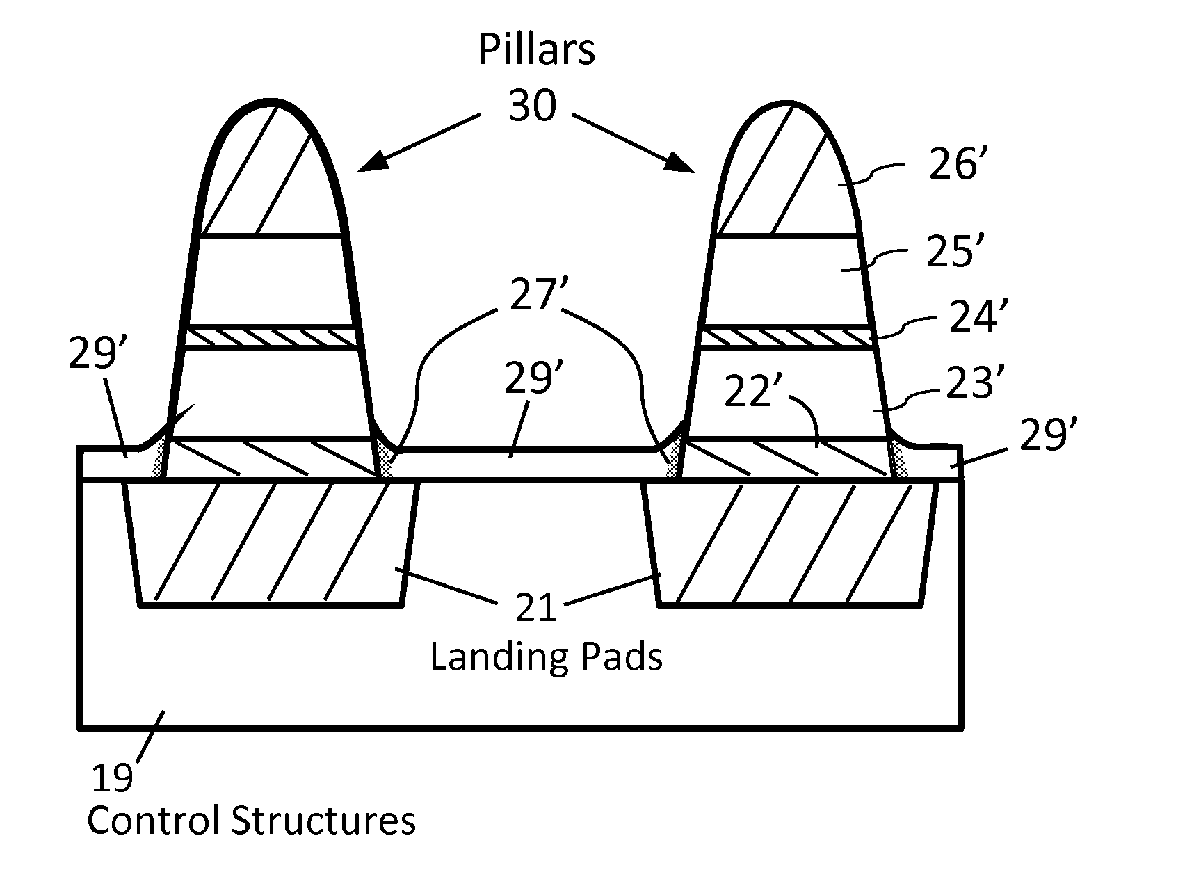
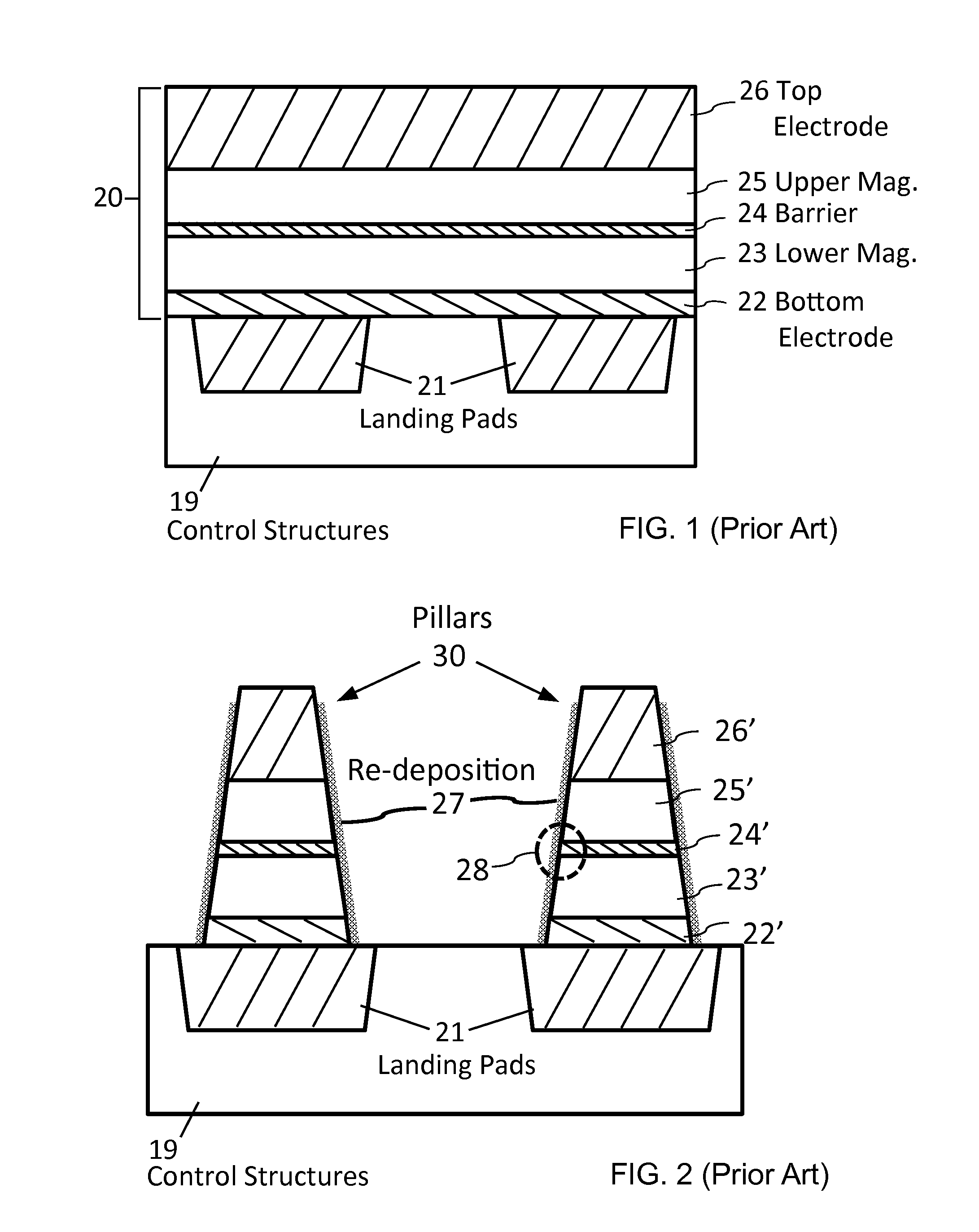
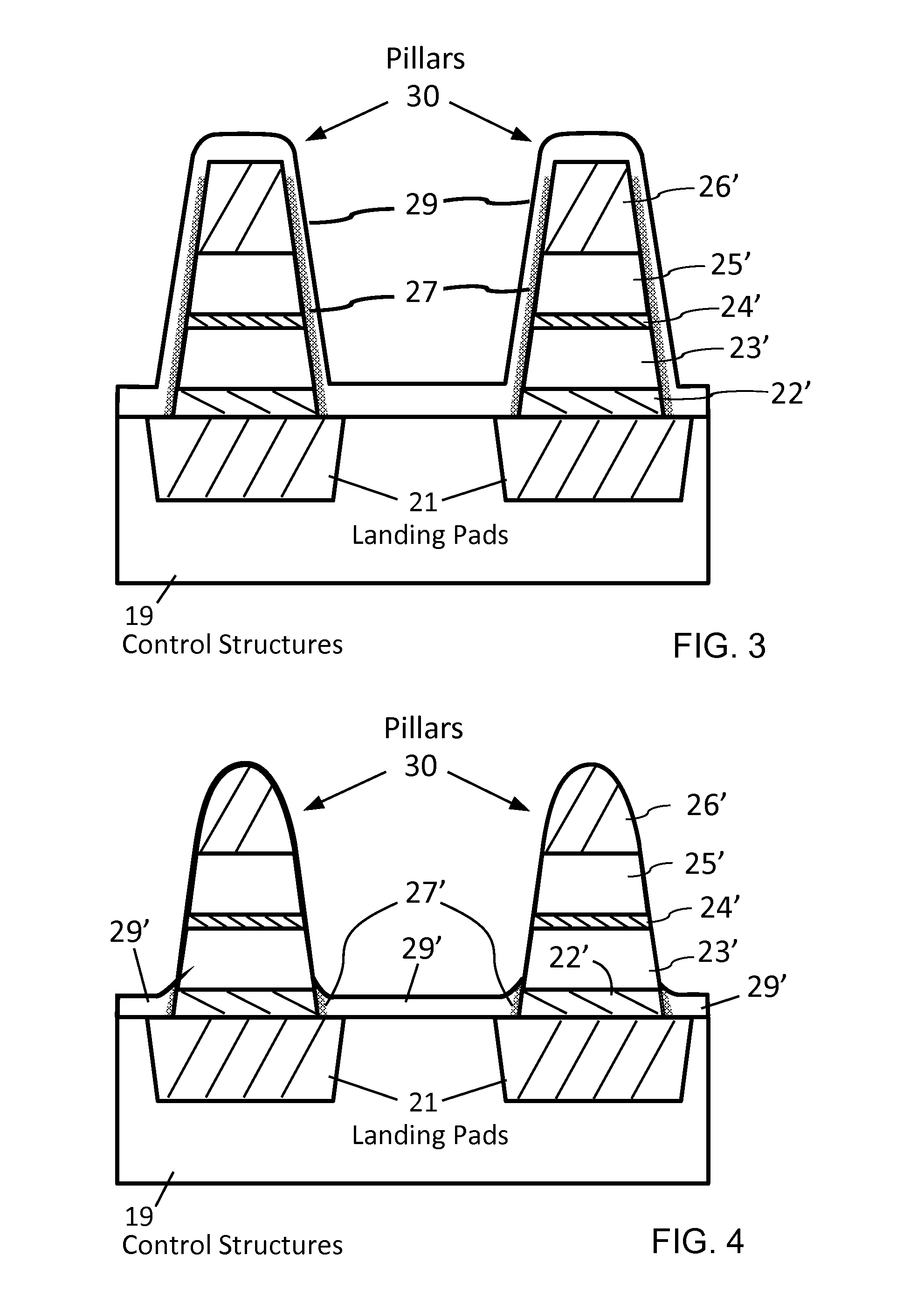
[0028]FIGS. 3-8 will be used to illustrate the first embodiment of the invention. The process stage in FIG. 3 follows that of FIG. 2. FIG. 3 illustrates the result of the deposition of dielectric film 29 over the pillars. The dielectric layer 29 has been formed over the MTJ pillars 30 by vertical directional deposition such as down-flow CVD or biased CVD. Accordingly the dielectric layer 29 is thicker in flat area such as the space between the pillars and is thinner on the sidewalls. The dielectric layer 29 completely covers the undesirable re-deposition material 27 and generally conforms to the existing topography of the pillars.

[0029]FIG. 4 illustrates a cross sectional view of a process stage, subsequent to that of FIG. 3, after sidewall cleaning has been performed using an etching technique that results in the top surface of the pillar being etched faster than the other surfaces which are etched isotropically. Although the dielectric material 29 on top of the pillars is th...

second embodiment

[0032]

[0033]FIGS. 9 and 10 illustrate a second embodiment of the invention which uses high density plasma CVD for sidewall cleaning. As for the first embodiment, the pillars are patterned as shown in FIG. 2. FIG. 9 shows that a relatively thick dielectric material 51 has been deposited over the pillars 30 which include metallic re-deposition material 27 on the sidewalls as described above. The dielectric material 51 is selected to be an oxygen-free material such as silicon nitride or silicon carbide. The dielectric material 51 is thinner on top of the pillars than in the valley areas between the pillars. Next a dry etching is used to etch the dielectric material 51 and re-deposition material 27. The chemistry system is selected for more rapid removal of the dielectric material 51 and slower removal of the material in the top electrode 26′. Appropriate systems include CH3OH and CO / NH3 and the like. The dielectric material 51 is vertically etched to the stage as shown in FIG. 10 and t...

third embodiment

[0034]

[0035]FIG. 11 to FIG. 13 illustrate a third embodiment of the invention that uses CMP for sidewall cleaning. The pillars are first patterned as illustrated in FIG. 2. FIG. 11 shows that a dielectric material 53 has been deposited over the pillars 30 in a relatively thin layer that roughly conforms to the topography of the pillars. The dielectric material 53 is selected to be an oxygen-free material such as silicon nitride or silicon carbide and like materials. The next part of the process is illustrated in FIG. 12 which shows that a relatively thick dielectric film 61, such as one of the silicon oxides, has been deposited and then the wafer has been planarized with CMP. Next the dielectric layers 53, 61 are vertically etched. The chemistry system is selected to have high selectivity for more rapid removal of the dielectric material 53, 61 and slower removal of the material in the top electrode 26′. Appropriate systems include CH3OH and CO / NH3 and the like.

[0036]The dielectric ...


PUM


Abstract

Fabrication methods for MRAM are described wherein any re-deposited metal on the sidewalls of the memory element pillars is cleaned before the interconnection process is begun. In embodiments the pillars are first fabricated, then a dielectric material is deposited on the pillars over the re-deposited metal on the sidewalls. The dielectric material substantially covers any exposed metal and therefore reduces sources of re-deposition during subsequent etching. Etching is then performed to remove the dielectric material from the top electrode and the sidewalls of the pillars down to at least the bottom edge of the barrier. The result is that the previously re-deposited metal that could result in an electrical short on the sidewalls of the barrier is removed. Various embodiments of the invention include ways of enhancing or optimizing the process. The bitline interconnection process proceeds after the sidewalls have been etched clean as described.

Description

FIELD OF THE INVENTION[0001]The present invention relates generally to fabrication methods for semiconductor Back-End-Of-Line (BEOL) memories including Magnetic Random Access Memory (MRAM) and more particularly to fabrication methods for MRAM that include ways of preventing interlayer shorting from metallic re-deposition material on sidewalls of the memory elements.BACKGROUND[0002]The BEOL memories such as RRAM (Resistive Random Access Memory), PRAM (Phase Change Random Access Memory), and MRAM have a resistive device as a memory element. These memories are expected to have wide application because of their high access speed and non-volatility at power-off.[0003]The memory device includes a multilayer magnetoresistive memory element in between a top electrode and a bottom electrode. The resistive memory element of MRAM is a Magnetic Tunnel Junction (MTJ) including a free layer and a fixed layer separated by a barrier layer. A magnetic moment of the free layer is manipulated by an el...

Claims


Application Information

Patent Timeline
IPC IPC(8): H01L21/02
CPCH01L27/222H01L43/12H01L43/08H10B61/00H10N50/01
Inventor SATOH, KIMIHIROHUAI, YIMINGZHOU, YUCHENZHANG, JINGJUNG, DONG HAABEDIFARD, EBRAHIMRANJAN, RAJIV YADAVKESHTBOD, PARVIZ
Owner AVALANCHE TECH
Why Eureka
Try Eureka