Method to realize flux free indium bumping

a technology of flux-free indium bumping and flux-free soldering, which is applied in the direction of semiconductor devices, semiconductor/solid-state device details, electrical apparatus, etc., can solve the problems of flux-free solder bumping, device performance degradation and even complete failure, and difficult to get a high-quality interconn

Inactive Publication Date: 2013-10-17
SHANGHAI INST OF MICROSYSTEM & INFORMATION TECH CHINESE ACAD OF SCI
View PDF2 Cites 4 Cited by
  • Summary
  • Abstract
  • Description
  • Claims
  • Application Information

AI Technical Summary

Benefits of technology

[0031]Reflow process is carried in an annealing furnace with

Problems solved by technology

For example, when using Sn solder to weld chips without flux, it will be very difficult to get a high quality interconnect due to the oxidized surface.
The pollution

Method used


Image

  • Method to realize flux free indium bumping
  • Method to realize flux free indium bumping

Examples


Embodiment Construction

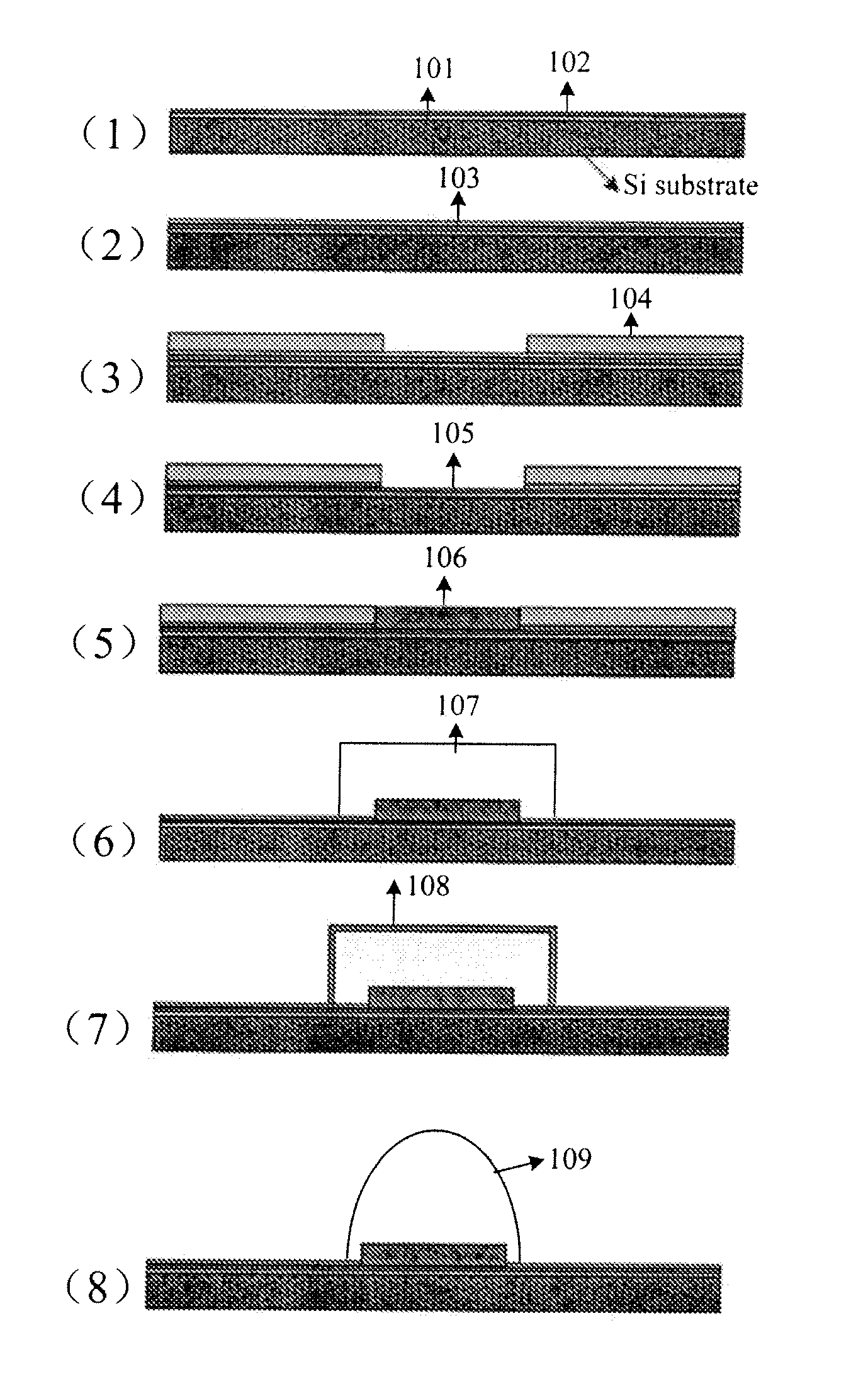
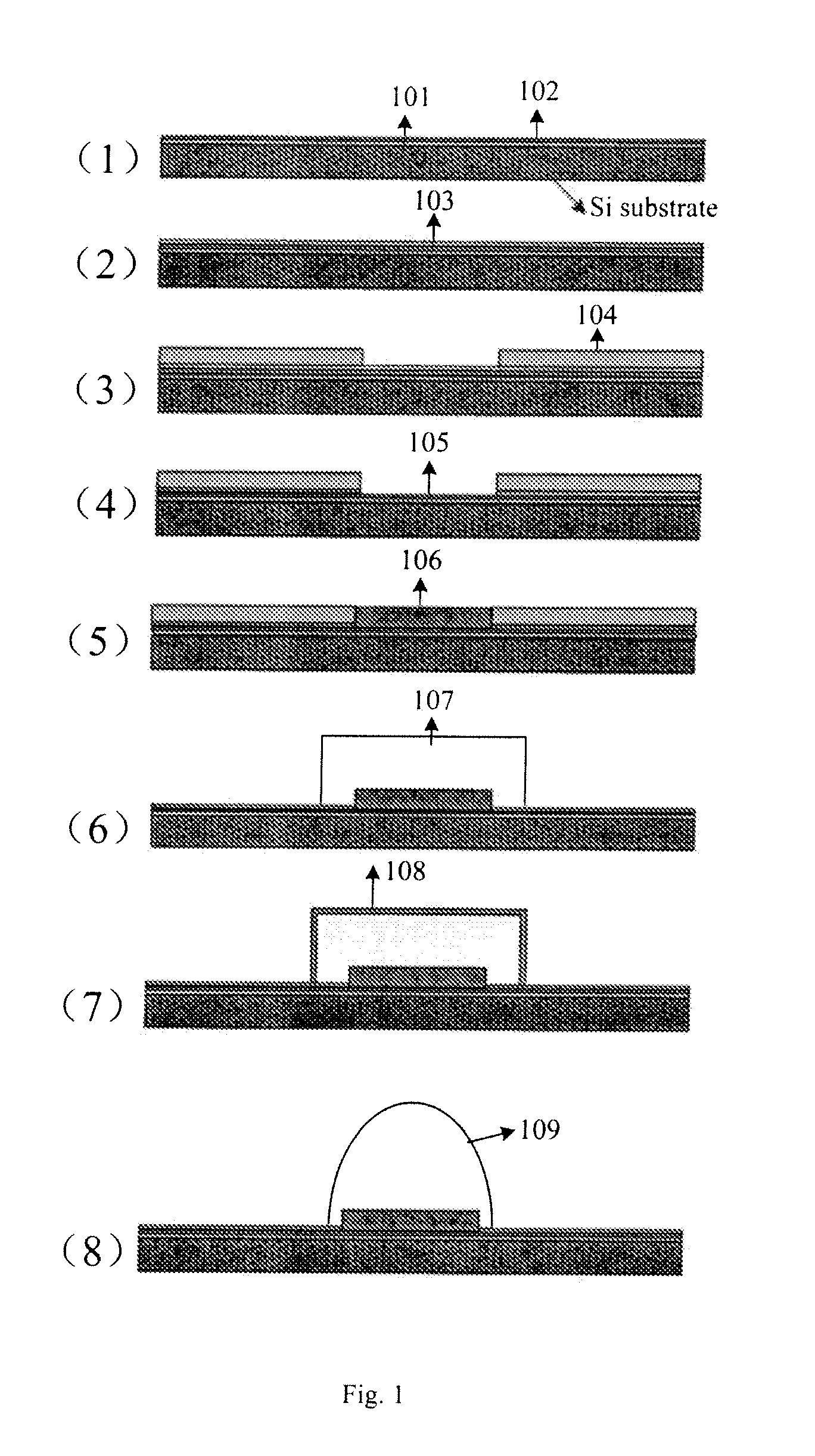
[0033]In order to clarify this invention, an example in detail can be described as following.

[0034]Step 1. Substrate plane preparation: 5000 Å SiO2 layer 101 is grown on the Si wafer substrate by thermal oxidation, and then a layer 102 is sputtered on the SiO2 layer. The Ti / Cu / Ti (200 Å / 2000 Å / 200 Å) used as underbump metallization (UMB) layer and also seed layer;

[0035]Step 2. Passivation layer preparation: A 5000 Å SiO2 layer 103 is prepared with plasma-enhanced chemical vapor deposition (PECVD) method;

[0036]Step 3. A 1.7 um positive photoreisit (S1912) 104 is coated on the wafer and then finish photography process;

[0037]Step 4. Contact hole opening: SiO2 and Ti on Cu layer are etched away with BOE (buffer-oxide-etch); 40 um Cu pattern 105 is exposed;

[0038]Step 5. Cu layer thickening: 2 um Cu 106 is prepared on sputtered Cu layer. After finishing Cu electroplating, photoresit is removed with acetone (the PR removal also can be carried in step 8 before the reflow process);

[0039]Step...


PUM

PropertyMeasurementUnit
Temperatureaaaaaaaaaa
Timeaaaaaaaaaa
Timeaaaaaaaaaa

Abstract

A method to realize flux free indium bumping process includes several steps including substrate metallization, contact holes opening, underbump metallization (UBM) layer thickening, indium bump preparation and Ag layer coating. The method can be used in the occasion for some special application, e.g., the packaging of the photoelectric chip (with optical lens), MEMS and biological detection chip, where the usage of flux is prohibited.

Description

BACKGROUND OF THE INVENTION[0001]1. Field of the Invention[0002]In this invention a method to realize fluxless indium bumping is described. This method can be used for the packaging for MEMS, photoelectric chip, bio-chip and so on. It is an invention in the field of microelectronics packaging.[0003]2. Prior Art[0004]Solder is a must for microelectronics packaging. Normally it can help to realize the signal transmission and provide mechanical support in and between chips. For a normal packaging process, flux is also a must. For example, when using Sn solder to weld chips without flux, it will be very difficult to get a high quality interconnect due to the oxidized surface. Such oxidized surface will prevent alloy formation when welding because it has a very high melting point. In order to get a high-quality interconnection, flux must be used for remove the oxide layer. But for some application, such as the packaging of the photoelectric chip (with optical lens), MEMS and biological d...

Claims


Application Information

Patent Timeline
IPC IPC(8): H01L23/00
CPCH01L24/11C25D3/46C25D3/54C25D5/02C25D5/10C25D5/50H01L24/03H01L24/05H01L24/13H01L24/94H01L2224/0345H01L2224/03462H01L2224/0347H01L2224/03849H01L2224/0401H01L2224/05082H01L2224/05083H01L2224/05147H01L2224/05166H01L2224/05666H01L2224/11462H01L2224/11502H01L2224/11825H01L2224/11849H01L2224/13099H01L2224/13109H01L2224/13562H01L2224/13639H01L2224/94H01L2924/01005H01L2924/01006H01L2924/01029H01L2924/01033H01L2924/01047H01L2924/01049H01L2924/0105H01L2924/01074H01L2924/01079H01L2924/01082H01L2924/01322H01L2924/014H01L2924/1461H01L2924/00014H01L2224/05647H01L2224/11H01L2924/00
Inventor HUANG, QIUPINGLUO, LEXU, GAOWEIYUAN, YUAN
Owner SHANGHAI INST OF MICROSYSTEM & INFORMATION TECH CHINESE ACAD OF SCI
Why Eureka
Try Eureka