
Sintered device

Inactive Publication Date: 2013-10-24
COMMONWEALTH SCI & IND RES ORG +1
View PDF4 Cites 34 Cited by
  • Summary
  • Abstract
  • Description
  • Claims
  • Application Information

AI Technical Summary

Benefits of technology

The present invention provides a method for making inorganic films with fewer defects and higher charge mobility compared with other solution-based methods. By treating the layers of nanoparticles between deposition steps, cracks and pinholes can be avoided, and an electronic device with power conversion efficiency greater than achieved before can be produced.

Problems solved by technology

A disadvantage of this single layer deposition approach is the formation of cracks and pinholes during the chemical treatment and the thermal annealing processes.
Accordingly, a lower quality device results.
This problematic occurrence of cracks and pinholes arises due to stresses that develop within the film as it contracts during either ligand exchange or during grain growth.
The effects of stress induced changes to nanocrystal films is one of the major limitations of single layer deposition of nanocrystals if chemical and thermal treatments are required.
In addition, solution processing typically leads to thinner devices than those which can be achieved through vacuum deposition.
Thinner devices tend to absorb less light, a drawback that is particularly significant for solar cells.
Accordingly, it is difficult to produce a sufficiently thick film of nanoparticles using single layer deposition and if a film of sufficient thickness can be achieved, stress induced cracks and pinholes limit the utility of devices comprising the film.

Method used


Image

  • Sintered device
  • Sintered device
  • Sintered device

Examples


examples

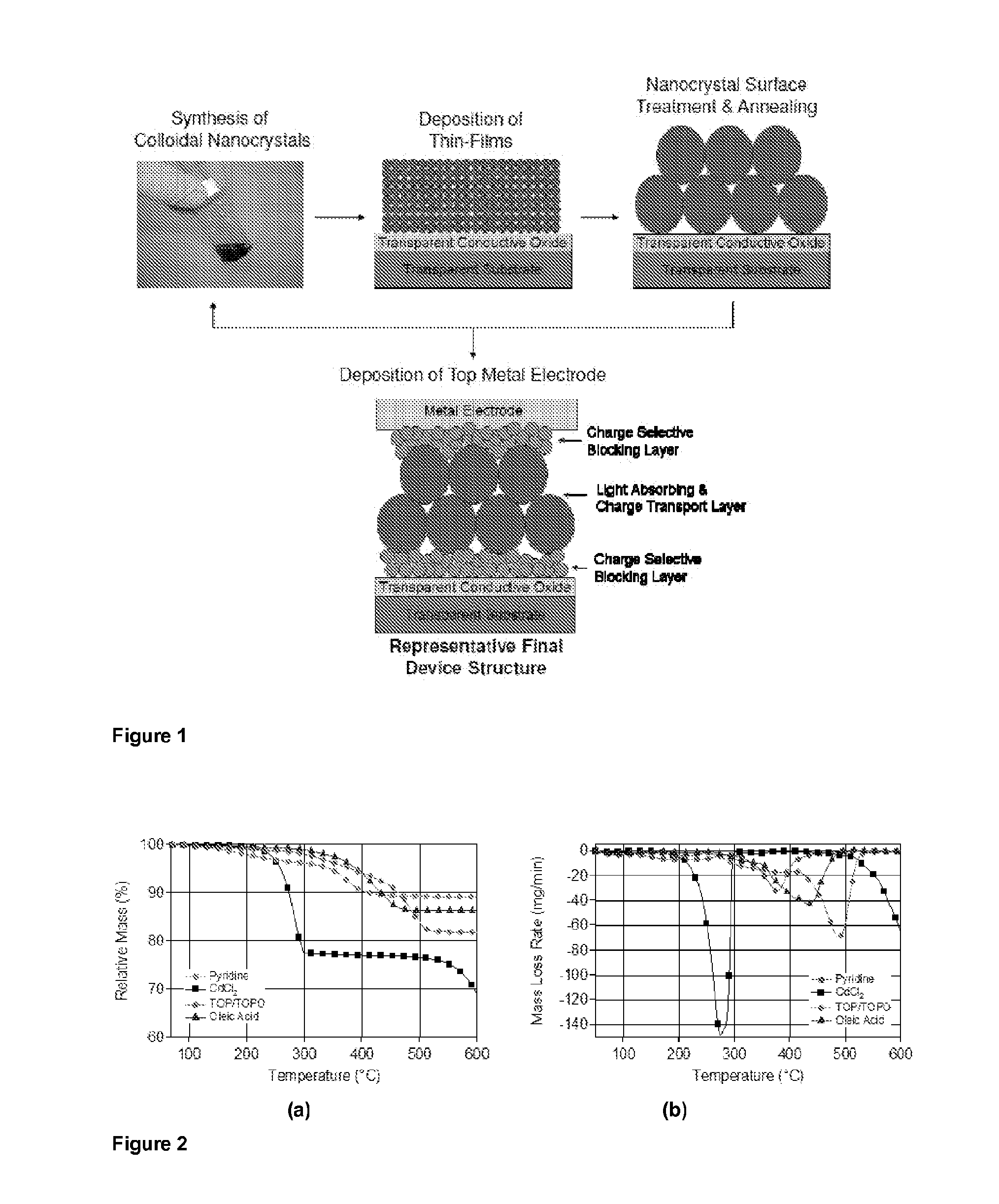
[0213]Layer-by-Layer approach to Solar Cell Fabrication

[0214]The general schematic for fabricating solution processed inorganic solar cells using a layer-by-layer technique is shown in FIG. 1. The technique begins by synthesizing a dispersion of nanoparticles of a required composition by any acceptable synthetic method which exists in the prior-art. The as synthesized nanoparticles, which are dispersed in their growth solution, are purified by filtration, centrifugation or extraction, and combinations thereof. Following purification, the surface chemistry of the nanoparticles may need to be changed to ensure dispersion in a solvent which is compatible with multi-layer deposition. The nature of the solvent may depend upon the exact treatment conditions of the deposited film, but is typically toluene, chloroform, chlorobenzene, hexane, xylene, pyridine, propanol, ethanol, methanol, methylethyl ketone, dimethylsulfoxide, dimethylforamide, or water or mixtures thereof.

[0215]Once the nan...


PUM


Abstract

A method for the production of an inorganic film on a substrate, the method comprising: (a) depositing a layer of nanoparticles on the substrate by contacting the substrate with a nanoparticle dispersion; (b) treating the deposited layer of nanoparticles to prevent removal of the nanoparticles in subsequent layer depositing steps; (c) depositing a further layer of nanoparticles onto the preceding nanoparticle layer on the substrate; (d) repeating treatment step (b) and deposition step (c) at least one further time; and (e) optionally thermally annealing the multilayer film produced following steps (a) to (d); wherein the method comprises at least one thermal annealing step in which the layer or layers of nanoparticles are thermally annealed.

Description

FIELD[0001]The present invention relates generally to electronic devices containing inorganic films of sintered nanoparticles, such as solar cells. The present invention also relates to methods for the production of such inorganic films on substrates, for the manufacture of such electronic devices.BACKGROUND[0002]A number of electronic devices contain inorganic films which provide electrical activity in the device. As one example, inorganic solar cells contain active inorganic material films of a charge accepting and a charge transporting material.[0003]Electronic devices such as solar cells and light-emitting diodes are typically manufactured by vacuum deposition of the active inorganic material film onto a substrate. Vacuum deposition involves depositing layers of particles onto the substrate at sub-atmospheric pressures.[0004]Another method for depositing particles onto a substrate involves a technique known as solution processing or solution deposition. Producing a device throug...

Claims


Application Information

Patent Timeline
IPC IPC(8): H01L31/18
CPCH01L31/18B82Y30/00B82Y40/00H01L21/02469H01L21/02521H01L21/02551H01L21/02601H01L21/02628H01L31/0296H01L31/02966H01L31/07H01L31/073H01L31/1828H01L31/1832H01L31/1864Y02E10/543Y02P70/50
Inventor JASIENIAK, JACEKMACDONALD, BRANDONMULVANEY, PAUL
Owner COMMONWEALTH SCI & IND RES ORG
Learn More