Fused polycyclic heteroaromatic compound, organic thin film including compound and electronic device including organic thin film
- Summary
- Abstract
- Description
- Claims
- Application Information
AI Technical Summary
Benefits of technology
Problems solved by technology
Method used
Image
Examples
example 1
Preparation of Fused Polycyclic Heteroaromatic Compound
[0105]The fused polycyclic heteroaromatic compound is synthesized as shown in the following Reaction Scheme 2.
[0106]Synthesis of Compound 1:
[0107]Benzodithiophene (5.29 g, 28 mmol) is dissolved in 100 mL of dry THF (tetrahydrofuran), the resultant is added to 100 mL of an anhydrous diethyl ether solution including butyl lithium (25 mL of 2.5 M in hexane solution) cooled at 0° C. in a dropwise fashion, a temperature is increased slowly, and the resultant is agitated at room temperature for 2 hours. 3-bromo-thieno[3,2:b]thiophene-2-aldehyde (12 g, 62 mmol) is added to the turbid solution in a dropwise fashion and is agitated overnight. 100 ml of an ammonium chloride saturated aqueous solution is added thereto, precipitated materials are filtered, and the resultant is washed with water and diethyl ether to obtain a compound 1 (yield: 70%).
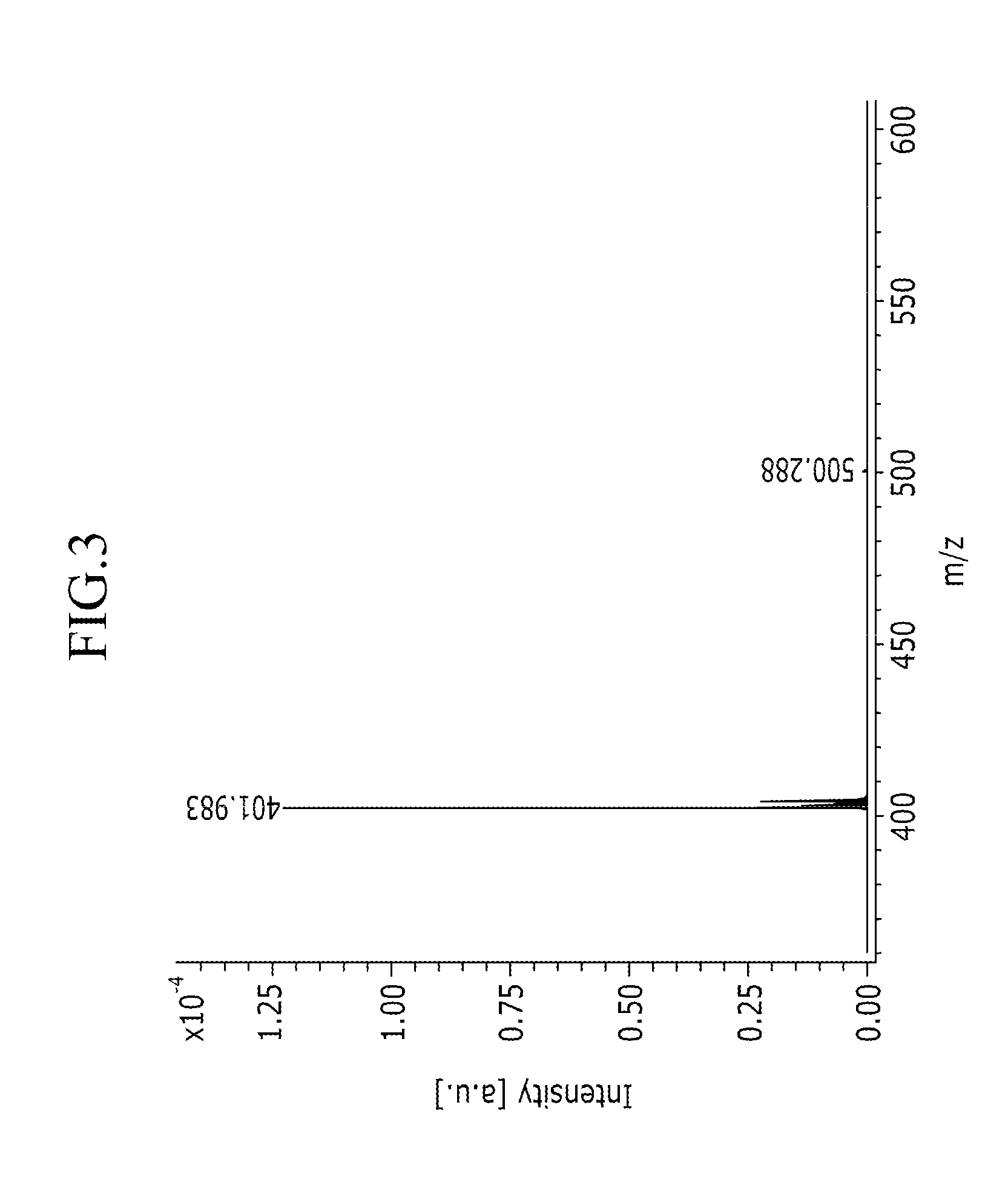
[0108]1H NMR (300 MHz, CDCl3): δ ppm 8.11 (d, 2H), 7.32 (d, 2H), 7.27 (d, 2H), 6.98 (d, 2H), 6...
example 2
Manufacture of Organic Thin Film Transistor Using Fused Polycyclic Heteroaromatic Compound
[0118]A silicon substrate covered with a 3000 Å silicon oxide film is rinsed with isopropyl alcohol for 10 minutes
[0119]The rinsed silicon substrate is treated with oxygen plasma, dipped in a octadecyl trichlorosilane solution that is diluted to a 5 mM concentration in hexane, for 30 minutes, is rinsed with hexane and ethanol, baked at 120° C. for 30 minutes, and washed with an ultrasonic wave in a chloroform solution. The washed silicon substrate is dried and the fused polycyclic heteroaromatic compound 4 according to Example 1 is applied at a thickness of 700 Å using a vacuum thermal deposition. Gold (Au) as a source-drain electrode is sputtered at a thickness of 1000 Å thereon to fabricate an OTFT device.
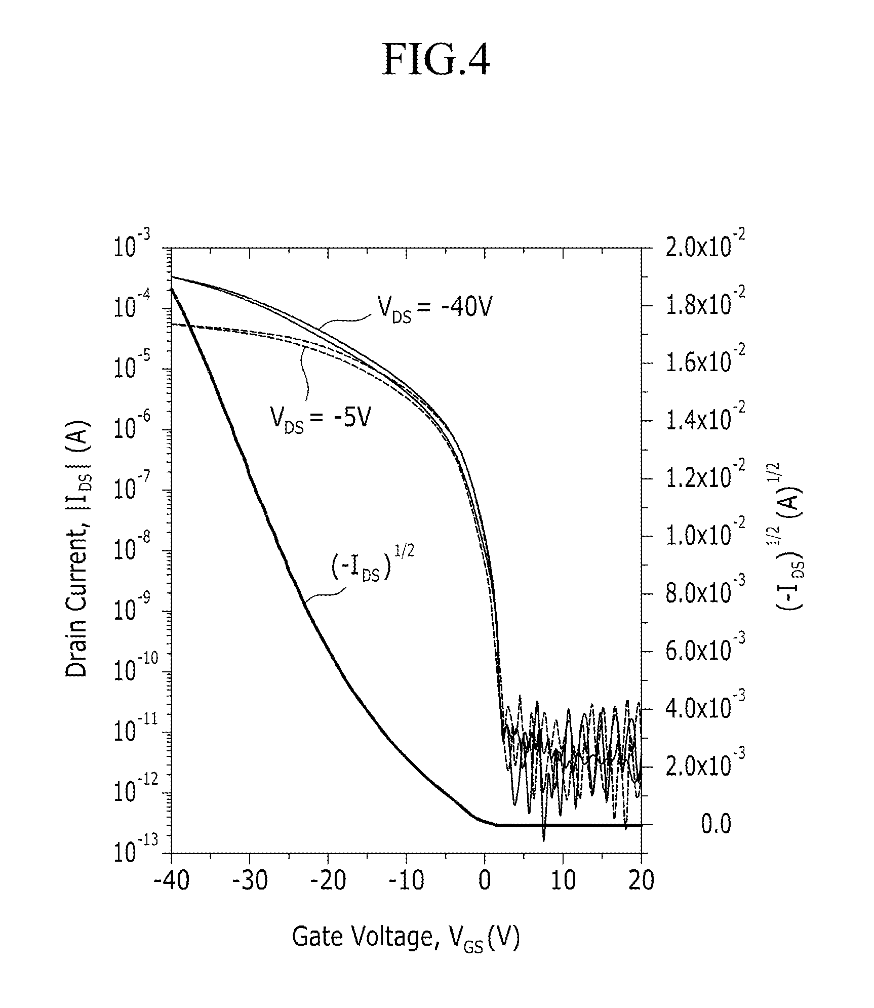
[0120]Current transfer characteristics of the OTFT device according to Example 2 is measured using a semiconductor characterization system (KEITHLEY, 4200-SCS) and the results are shown in F...
PUM
 Abstract
Description
Claims
Application Information


