
Method of laser irradiation, laser irradiation apparatus, and method of manufacturing a semiconductor device

a laser irradiation and laser irradiation technology, applied in semiconductor lasers, manufacturing tools, instruments, etc., can solve the problems of reducing throughput, reducing reducing so as to reduce the optical path length of the optical system, improve the efficiency of the manufacturing process, and facilitate the effect of optical adjustmen

Inactive Publication Date: 2013-12-05
SEMICON ENERGY LAB CO LTD
View PDF0 Cites 0 Cited by
  • Summary
  • Abstract
  • Description
  • Claims
  • Application Information

AI Technical Summary

Benefits of technology

The present invention aims to provide a laser irradiation apparatus with a short optical path length that can avoid deviation of a convergent position at both ends of a rectangular beam, particularly a linear beam, in a long-dimension direction. The invention is useful for reducing the optical path length of the optical system to enable easy optical adjustment and for forming the laser beam corresponding to the length of a large area substrate. Annealing uniformity is important for ensuring uniform properties of the substrate and the resulting semiconductor device. The technical effects include improved operational characteristics and reliability of the semiconductor device manufactured from theseTFTs.

Problems solved by technology

It is extremely difficult and requires a large footprint to perform optical adjustment of the optical system with such a long optical path length, thereby causing a problem in that the apparatus becomes larger.
If such a linear beam is used to perform annealing on an irradiation subject, annealing can not be uniformly performed.
For example, in case of performing annealing on a large area substrate, if the linear beam of 300 mm in the length direction is used, it is impossible to perform annealing on the entire surface of the large area substrate with only one scanning by irradiating the linear beam to the large area substrate while moving the beam in one direction relative to the substrate, and it is required to move the beam in at least two directions or to irradiate the beam plural times, thereby reducing the throughput.
As a result, depending on a scanning method of the laser beam, there is formed a region where annealing is performed plural times or a region where no annealing is performed, so that there is a strong possibility that the annealing is not uniformly performed.
Even if the linear beam is made longer in the length direction in order to perform annealing uniformly, as long as such a linear beam with the convergent position deviating at both ends in the length direction is used, annealing can not be uniformly performed.

Method used


Image

  • Method of laser irradiation, laser irradiation apparatus, and method of manufacturing a semiconductor device
  • Method of laser irradiation, laser irradiation apparatus, and method of manufacturing a semiconductor device
  • Method of laser irradiation, laser irradiation apparatus, and method of manufacturing a semiconductor device

Examples


embodiment 1

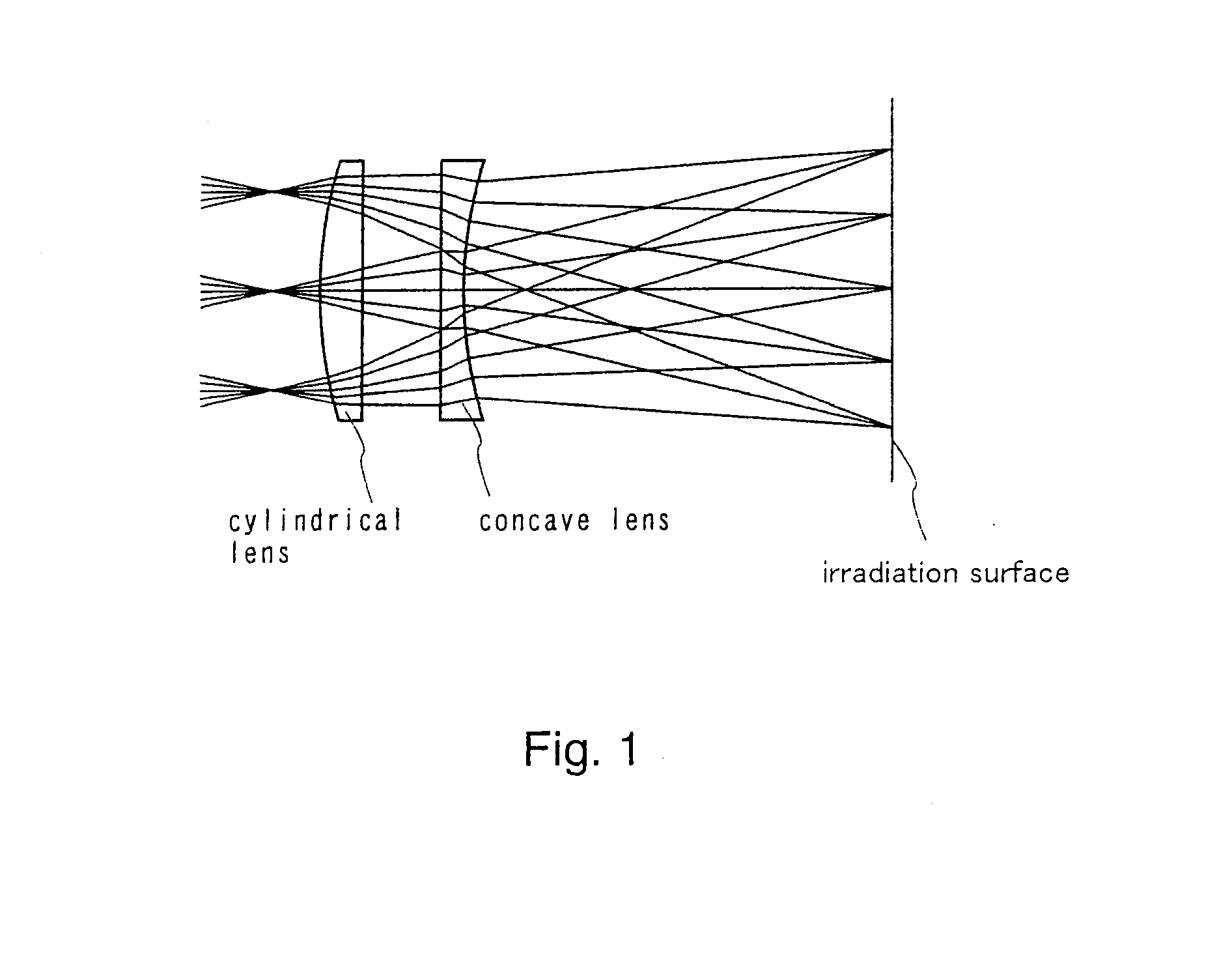
[0074]In this embodiment, an example of applying the present invention is described in the case that an optical path length of an optical system which forms a laser beam into a linear shape is made smaller. In addition, in an explanation of an arrangement of lenses, a travel direction of photon at an optical axis of a laser beam indicates forward.

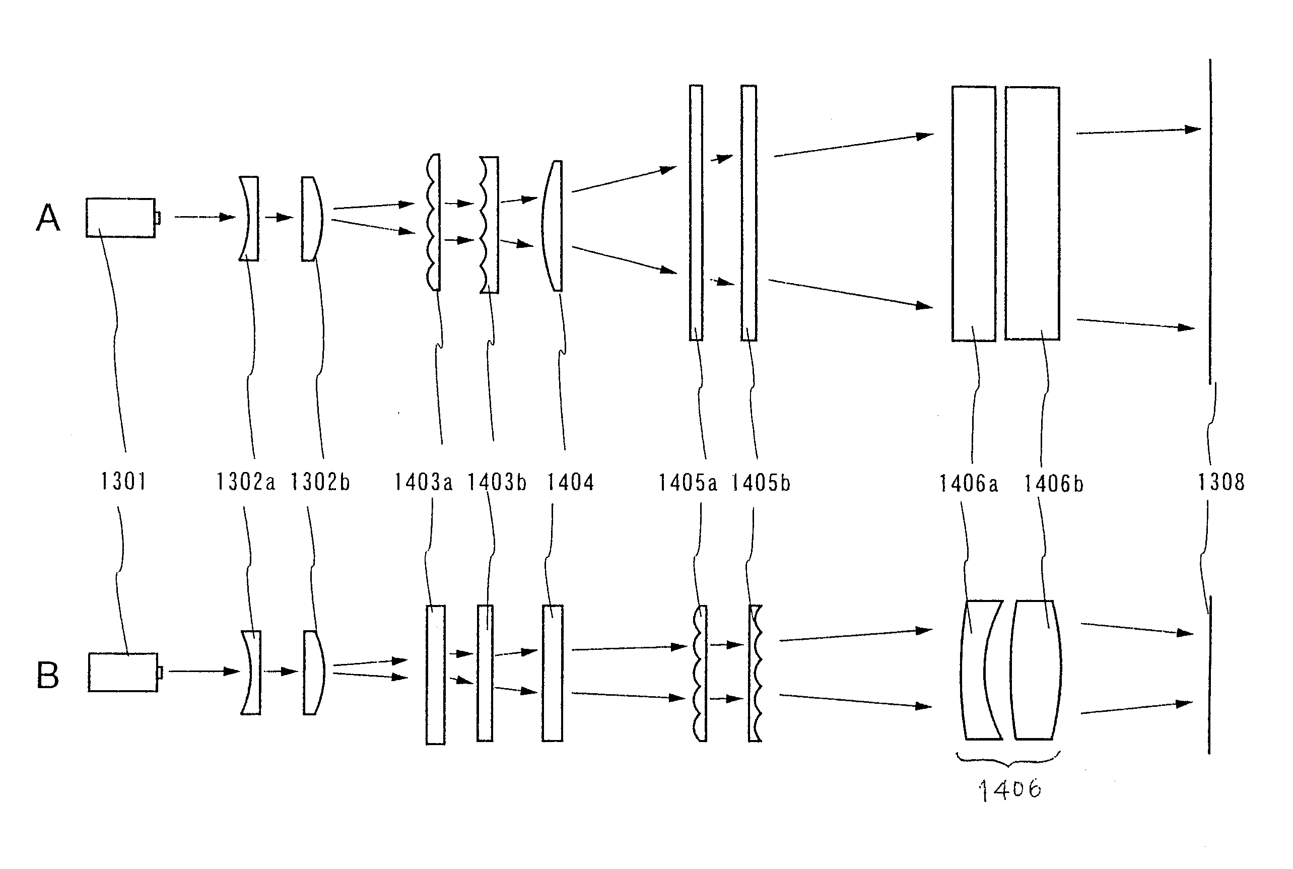
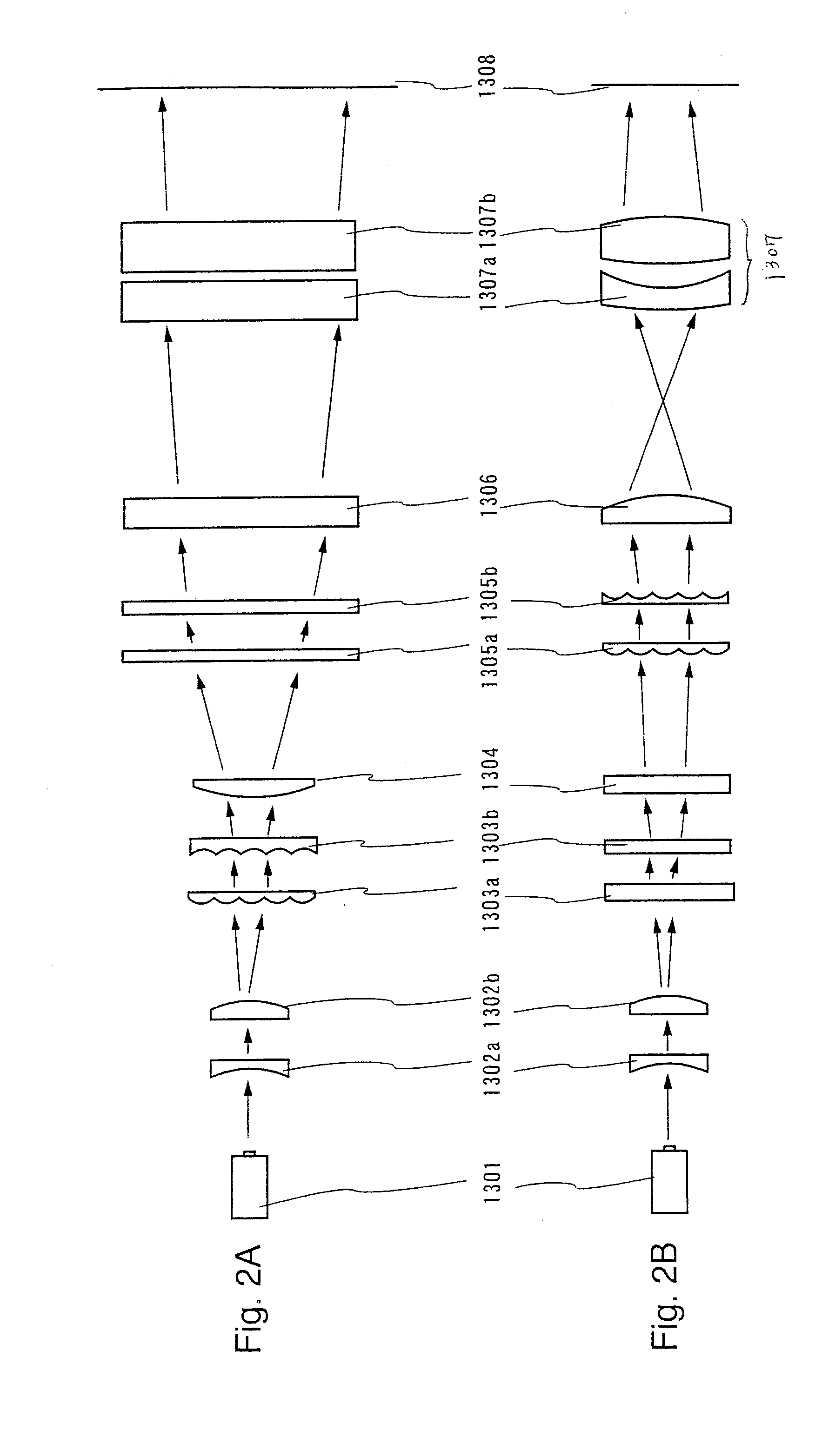
[0075]First, an optical system having a 5065.2 mm in an optical path length for forming a linear beam having a 300 mm in longitudinal direction is illustrated. FIG. 2A shows an optical system in the case where a longitudinal direction of laser beam is viewed from a direction perpendicular thereto and FIG. 2B shows the optical system in the case where a width direction of laser beam is viewed from a direction perpendicular thereto.

[0076]Laser beam emitted from a laser 1301 is expanded by a beam expander in both the longitudinal direction and the width direction by about two times. The beam expander is composed of a spherical lens (50 mm in r...

embodiment 2

[0089]In Embodiment 1, a deviation of a convergent position is avoided by providing the second lens 1406b of the doublet cylindrical lens instead of the troidal lens. In this embodiment, a method that a deviation of a convergent position is corrected by newly adding one cylindrical lens, without changing the form of the doublet cylindrical lens 1406 is described with reference FIG. 9. FIG. 9A shows an optical system in the case where a longitudinal direction is viewed from a direction perpendicular thereto and FIG. 9B shows the optical system in the case where a width direction is viewed from a direction perpendicular thereto.

[0090]A cylindrical lens 1507 is added at a distance of 40 mm from the doublet cylindrical lens 1406 in the optical system (FIGS. 4A and 4B) shown in Embodiment 1. The cylindrical lens 1507 has 400 mm in length, 70 mm in width, 20 mm in thickness, R1=∞, and R2=7000 mm (preferably 4000 to 10000 mm). The cylindrical lens 1507 is arranged such that the curvature i...

embodiment 3

[0091]In this embodiment, an example of an optical system in order to form a linear beam having 1000 mm in length in the longitudinal direction on an irradiation surface. FIG. 11A shows an optical system in the case where a longitudinal direction is viewed from a direction perpendicular thereto and FIG. 11B shows the optical system in the case where a width direction is viewed from a direction perpendicular thereto.

[0092]Laser beam emitted from a laser 1301 is expanded by a beam expander in both the longitudinal direction and the width direction by about two times. The beam expander is composed of a spherical lens (50 mm in radius, 7 mm in thickness, R1=−220 mm, and R2=∞) 1302a and a spherical lens (50 mm in radius, 7 mm in thickness, R1=∞, and R2=−400 mm) 1303b which is located at a distance of 400 mm from the spherical lens 1302a.

[0093]The cylindrical lens array 1003 includes 40 cylindrical lenses (each having 150 mm in length, 2 mm in width, 5 mm in thickness, R1=4 mm, and R2=∞)...


PUM

PropertyMeasurementUnit
lengthaaaaaaaaaa
aspect ratioaaaaaaaaaa
sizeaaaaaaaaaa

Abstract

If an optical path length of an optical system is reduced and a length of a laser light on an irradiation surface is increased, there occurs curvature of field which is a phenomenon that a convergent position deviates depending on an incident angle or incident position of a laser light with respect to a lens. To avoid this phenomenon, an optical element having a negative power such as a concave lens or a concave cylindrical lens is inserted to regulate the optical path length of the laser light and a convergent position is made coincident with a irradiation surface to form an image on the irradiation surface.

Description

BACKGROUND OF THE INVENTION[0001]1. Field of the Invention[0002]The present invention relates to a laser beam irradiation method and a laser irradiation apparatus for using the method (apparatus including a laser and an optical system for guiding laser beam emitted from the laser to an object to be irradiated). In addition, the present invention relates to a method of manufacturing a semiconductor device, which includes a laser beam irradiation step. Note that a semiconductor device described here includes an electro-optical device such as a liquid crystal display device or a light-emitting device and an electronic device that includes the electro-optical device as a part.[0003]2. Description of the Related Art[0004]In recent years, a wide study has been made on a technique in which laser annealing is performed for a semiconductor film formed on an insulating substrate made of glass or the like, to crystallize the film, to improve its crystallinity so that a crystalline semiconducto...

Claims


Application Information

Patent Timeline
Patent Type & Authority Applications(United States)
IPC IPC(8): H01L33/08G02B27/18B23K26/06B23K26/073B23K26/08B23K26/082B23K101/40G02B27/09G02F1/37H01L21/20H01L21/265H01L21/268H01L21/77H01L21/84H01L27/32H01L51/52H01S3/00H01S5/40
CPCH01L33/08B23K26/0604B23K26/0732B23K26/0736B23K26/0738G02B27/09G02B27/095H01L21/268H01S3/005H01S5/4012H01S5/4025H01L27/1285H01L21/02683H01L21/02532H01L21/02686H01L21/02422H01L21/02678H10K59/122H10K59/12H10K59/87B23K26/064B23K26/06H10K50/84H10K50/8426H01L21/28017G02B27/0955
Inventor TANAKA, KOICHIROMORIWAKA, TOMOAKI
Owner SEMICON ENERGY LAB CO LTD
Learn More