Oscillator

Active Publication Date: 2013-12-12
CANON KK
View PDF4 Cites 26 Cited by
  • Summary
  • Abstract
  • Description
  • Claims
  • Application Information

AI Technical Summary

Benefits of technology

[0009]According to the exemplary embodiment of the present invention, a low-impedance circuit for suppressing parasitic oscillation can be disposed at any position in a microstrip resonator at which t

Problems solved by technology

Thus, it has not been easy to d

Method used


Image

  • Oscillator
  • Oscillator
  • Oscillator

Examples


first embodiment

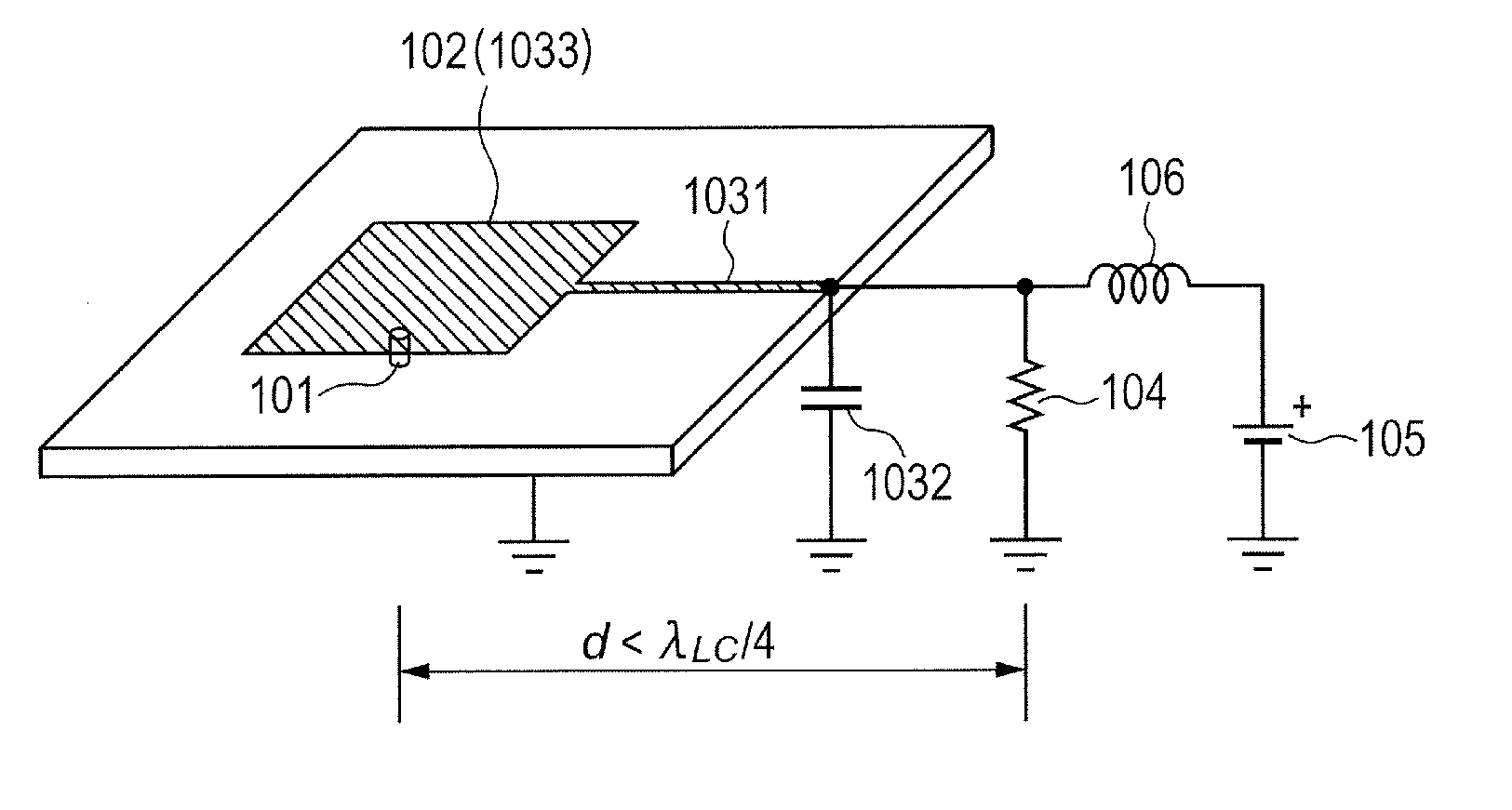
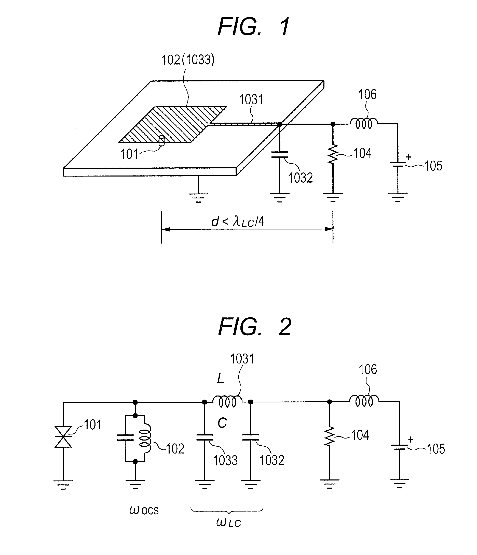
[0020]An oscillator according to a first embodiment of the present invention is now described with reference to FIGS. 1 and 2. FIG. 1 is a schematic diagram illustrating the oscillator of this embodiment. FIG. 2 is a circuit diagram illustrating the oscillator of this embodiment. In this embodiment, a resonant tunneling diode (RTD), an Esaki diode, or a Gunn diode is typically selected as a negative resistance device 101. Otherwise, a transistor having one terminated lead may be used. A resonator 102 for defining an oscillation frequency of an electromagnetic wave excited by the negative resistance device is a microstrip resonator using a patch antenna or a microstrip line with a finite length. The microstrip resonator refers to a resonator including an electrically floating conductive layer such as a metal plate connected to the ground. In FIG. 2 illustrating a corresponding equivalent circuit, devices are discriminated between the resonance circuit 102 for an oscillation frequency...

example 1

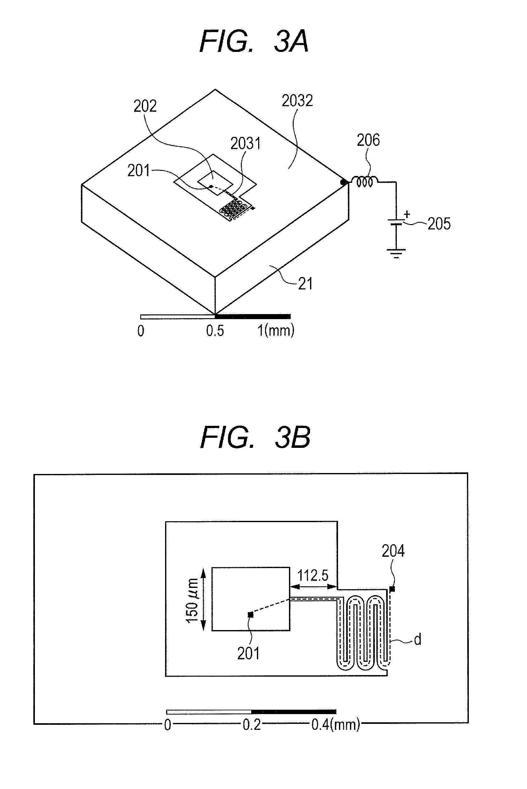
[0027]An oscillator according to Example 1 of the present invention is now described with reference to FIGS. 3A and 3B. FIG. 3A is a perspective view illustrating the oscillator of Example 1. FIG. 3B is a top view illustrating metal patterning in the vicinity of a patch antenna. In Example 1, a resonant tunneling diode (RTD) is used as a negative resistance device.

[0028]FIGS. 3A and 3B illustrate the patch antenna formed of metal patterning for electromagnetic wave oscillation and its peripheral circuit structure. The patch antenna of Example 1 is an oscillator for oscillating at approximately 0.5 THz. An RTD 201 includes, for example, a multiple quantum well structure of InGaAs / InAlAs and InGaAs / AlAs and electrical contact layers of n-InGaAs which are formed on an InP substrate 21. For example, a triple-barrier structure is used as the multiple quantum well structure. More specifically, a semiconductor multi-layer structure of AlAs (1.3 nm) / InGaAs (7.6 nm) / InAlAs (2.6 nm) / InGaAs (5...

example 2

[0033]An oscillator according to Example 2 of the present invention is now described with reference to FIGS. 4A and 4B. FIGS. 4A and 4B are diagrams illustrating an oscillator according to a modified example of Example 1, exemplifying the case where a resonant tunneling diode is used as a negative resistance device also in Example 2 and the oscillation frequency is high. FIG. 4A is a perspective view of the oscillator of Example 2. FIG. 4B is a top view illustrating metal patterning in the vicinity of a patch antenna.

[0034]The patch antenna of Example 2 is an oscillator for oscillating at approximately 0.9 THz. The details of the patterning are illustrated in FIG. 4B. A patch 302 is 75 μm in length on a side in the resonance direction. Taking into account the reactance of the RTD of 2 μm in diameter that is connected to the bottom of the patch 302, the oscillation frequency is approximately 0.9 THz. Even when the length of the side of the resonator is halved, the oscillation frequen...


PUM


Abstract

An oscillator configured to oscillate an electromagnetic wave, including: a negative resistance device; a microstrip resonator configured to determine an oscillation frequency of an electromagnetic wave excited by the negative resistance device; a resistance device and a capacitance device, which form a low-impedance circuit configured to suppress parasitic oscillation; and a strip conductor configured to connect the capacitance device of the low-impedance circuit and the microstrip resonator to each other, in which an inductance L of the strip conductor and a capacitance C of the microstrip resonator produce a resonance frequency of ½π√LC, and ¼ of an equivalent wavelength of the resonance frequency is larger than a distance between the negative resistance device and the resistance device of the low-impedance circuit via the strip conductor, is provided.

Description

BACKGROUND OF THE INVENTION[0001]1. Field of the Invention[0002]The present invention relates to an oscillator using a negative resistance device, and more particularly, to an electromagnetic-wave oscillator for a frequency band in a range of, for example, from a millimeter band to a terahertz band (30 GHz or higher and 30 THz or lower; the same applies hereinafter).[0003]2. Description of the Related Art[0004]As is widely recognized, a negative resistance device, together with a resonator, is useful in application fields of oscillators for electromagnetic waves. It has heretofore been known to generate an electromagnetic wave containing at least a part of frequency components in a frequency band in a range of from a millimeter band to a terahertz band (hereinafter also simply referred to as “terahertz wave and the like”). As an example, IEEE Electron Device Letters, Vol 18, 218 (1997) discloses an oscillator in which a negative resistance device is monolithically integrated on a su...

Claims


Application Information

Patent Timeline
IPC IPC(8): H03B5/30
CPCH03B5/30H03B7/14H03B2200/0032H03B2200/0084
Inventor SEKIGUCHI, RYOTA
Owner CANON KK
Why Eureka
Try Eureka