Method of manufacturing a flexible substrate having metal wiring embedded therein,and flexible substrate manufactured by the method

a manufacturing method and technology of flexible substrate, applied in the direction of non-metallic protective coating applications, conductive pattern formation, chemistry apparatus and processes, etc., can solve the problems of complex process, difficult verification of wiring defect generation during manufacturing process, and difficult formation of multi-layer circuit substrates, etc., to achieve low resistance

Active Publication Date: 2014-01-02
KOREA INST OF MATERIALS SCI
View PDF0 Cites 22 Cited by
  • Summary
  • Abstract
  • Description
  • Claims
  • Application Information

AI Technical Summary

Benefits of technology

[0067]According to the method of manufacturing a metal wiring buried flexible substrate, a metal wiring may be inserted into the flexible substrate by using a sacrificial layer made by using a polymer soluble in water or an organic solvent or a photodegradable polymer, and a wiring having a low resistance irrespective of the height of the metal wiring may be formed. In addition, through separating the metal wiring buried flexible substrate from the substrate by removing the sacrificial layer using water or an organic solvent, or the light, the metal wiring buried flexible substrate may be clearly separated from the substrate.

Problems solved by technology

However, a very complicated process is necessary for manufacturing the multi-layer circuit patterns on the circuit substrate, and the verification of the generation of a wiring defect during performing the manufacturing process may be difficult.
Particularly, for a recently developed wafer level package, in which a circuit wiring may be directly formed on a semiconductor chip, the formation of a multi-layer circuit substrate may be very difficult because the area of the wafer level package is very small.
Meanwhile, the width of the wiring becomes narrower to form a large number of more complicated wirings on a substrate.
With respect to method (1), the development of a material having a lower specific resistance than that of widely used copper, aluminum or silver may be difficult.
With respect to method (2), practical application may be difficult concerning a circuit designing matter.
According to the above-described common methods, lots of materials may be consumed, and the process may be conducted through various steps including deposition, patterning, etching, etc and may be complicated.
However, when the inorganic separator is used, the separation of the wiring and the member may not be easily performed while conducting the separating process of the member and the metal wiring from the substrate.
That is, the metal wiring of the wiring substrate may be incompletely separated from the substrate even though using the separator.

Method used


Image

  • Method of manufacturing a flexible substrate having metal wiring  embedded therein,and flexible substrate manufactured by the method
  • Method of manufacturing a flexible substrate having metal wiring  embedded therein,and flexible substrate manufactured by the method
  • Method of manufacturing a flexible substrate having metal wiring  embedded therein,and flexible substrate manufactured by the method

Examples


example 1

Manufacture of a Metal Wiring Buried Flexible Substrate 1

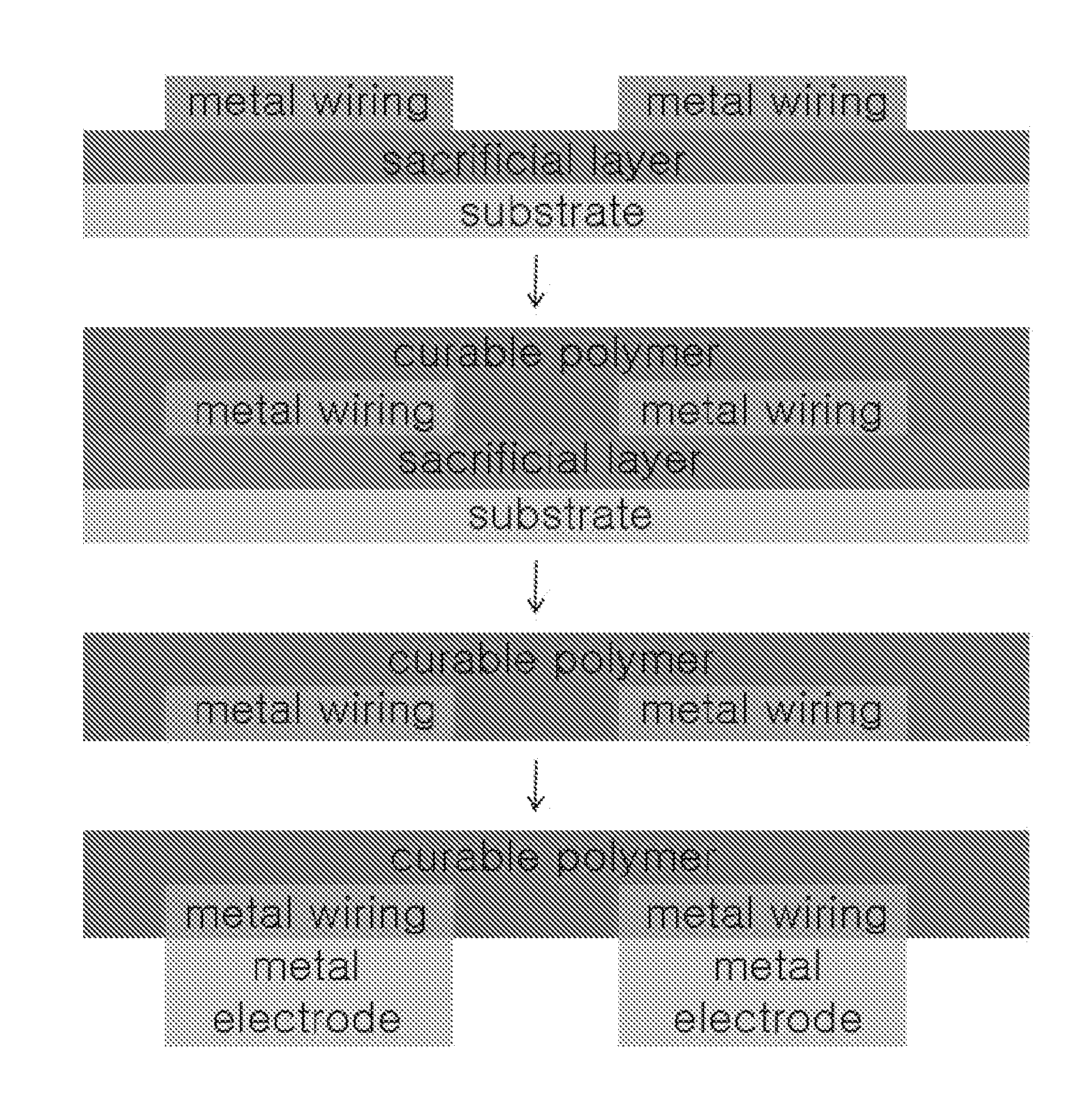
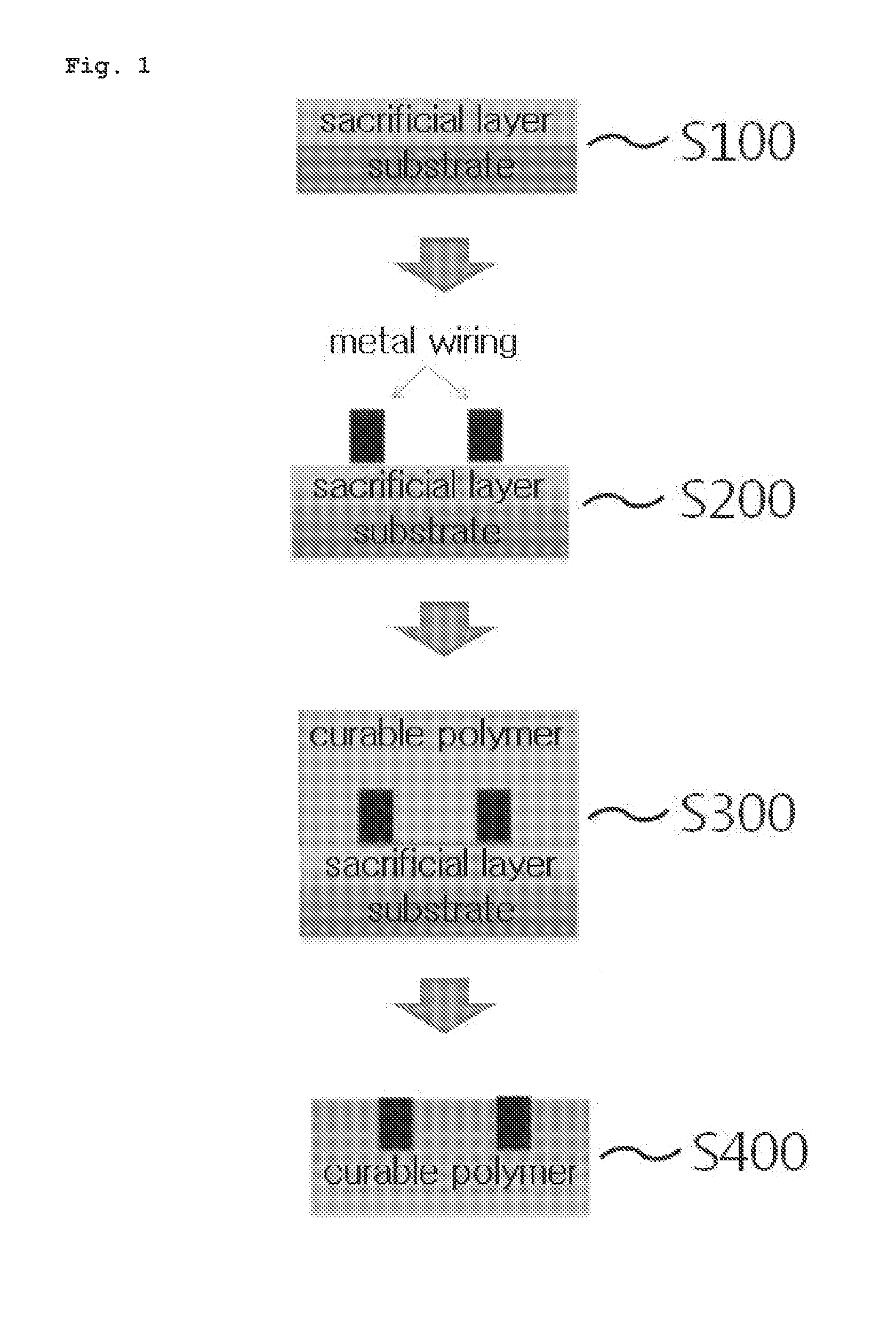
[0173]Step 1: After cleaning a glass substrate using acetone and isopropyl alcohol, an O2 plasma treatment (process condition: treatment at an O2 gas of 1 sccm, a process pressure of 10 mTorr, and a DC power of 500 W for 300 seconds) was conducted to modify the surface of the substrate to have a hydrophilic property. Into distilled water, polyvinyl alcohol (PVA, molecular weight: 90,000-120,000, 99% Sigma-Aldrich) was added by 10 wt % concentration to prepare a polyvinyl alcohol solution. This polyvinyl alcohol solution was coated on the glass substrate by a spin coating method (1,000 rpm for 50 seconds). After completing the coating, a thermal treatment was conducted on a hot-plate at 90° C. for 5 minutes to form a sacrificial layer having a thickness of about 700 nm.

[0174]Step 2: By using a gravure offset printing apparatus, an Ag paste (silver nano paste DGP, nano new material (ANP)) was coated on the sacrificial layer form...

example 2

Manufacture of a Metal Wiring Buried Flexible Substrate 2

[0177]Step 1: After cleaning a glass substrate using acetone and isopropyl alcohol, an O2 plasma treatment (process condition; treatment at an O2 gas of 1 sccm, a process pressure of 10 mTorr, and a DC power of 500 W for 300 seconds) was conducted to modify the surface of the substrate to have a hydrophilic property. Into distilled water, polyvinyl alcohol (PVA, molecular weight: 90,000-120,000, 99%, Sigma-Aldrich) was added by 10% concentration to prepare a polyvinyl alcohol solution. This polyvinyl alcohol solution was coated on the glass substrate by a spin coating method (1,000 rpm for 60 seconds). After completing the coating, a thermal treatment was conducted on a hot-plate at 90° C. for 5 minutes to form a sacrificial layer having a thickness of about 700 nm.

[0178]Step 2: By using a gravure offset printing apparatus, an Ag paste (silver nano paste DGP, nano new material (ANP)) was coated on the sacrificial layer formed ...

example 3

Manufacture of a Metal Wiring Buried Flexible Substrate 3

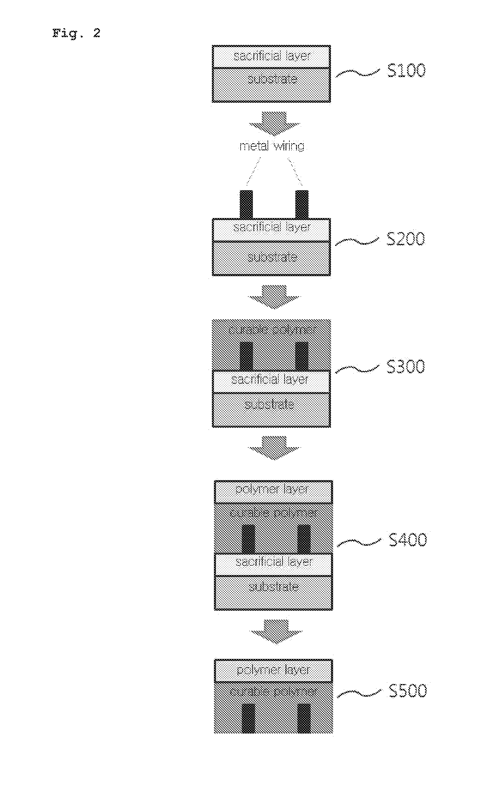
[0182]A metal wiring buried flexible substrate was manufactured by conducting the same procedure explained in Example 2 except for attaching a polyimide flexible substrate onto the polymer layer in Step 4 in Example 2.


PUM

PropertyMeasurementUnit
diameteraaaaaaaaaa
thicknessaaaaaaaaaa
thicknessaaaaaaaaaa

Abstract

Disclosed are a method of manufacturing a metal wiring buried flexible substrate and a flexible substrate manufactured by the same. The method includes coating a sacrificial layer including a polymer soluble in water or an organic solvent, or a photodegradable polymer on a substrate (Step 1), forming a metal wiring on the sacrificial layer in Step 1 (Step 2), forming a metal wiring buried polymer layer by coating a curable polymer on the sacrificial layer including the metal wiring formed thereon in Step 2 and curing (Step 3) and separating the polymer layer in Step 3 from the substrate in Step 1 by removing through dissolving in the water or the organic solvent or photodegrading only the sacrificial layer present between the substrate in Step 1 and the polymer layer in Step 3 (Step 4).

Description

TECHNICAL FIELD[0001]The present disclosure relates to methods of manufacturing a metal wiring buried flexible substrate and flexible substrates manufactured by the same.BACKGROUND ART[0002]Recently, various home appliances and electronic products have been developed in line with the technical development in electric industry and electronic industry. Most of the home appliances and the electronic products include a circuit substrate, into which an electric device, an electronic device and a semiconductor package may be inserted. The circuit substrate includes a circuit wiring for an electric connection of the electric device, the electronic device and the semiconductor package. Commonly used circuit wirings may be formed by patterning a metal layer formed on an insulating substrate. When the circuit wirings formed on the insulating substrate intersect on the same plane, a short between the circuit wirings may be generated. Thus, a common circuit substrate may include multi-layer cir...

Claims


Application Information

Patent Timeline
Patent Type & Authority Applications(United States)
IPC IPC(8): H05K3/10H05K1/02
CPCH05K3/10H05K1/02H05K1/0393H05K3/207H05K3/246H05K2201/0376Y10T29/49156B32B15/08H05K3/28H05K3/0017
Inventor KANG, JAE WOOKKIM, DO GEUNKIM, JONG KUKJUNG, SUNG HUNSONG, MYUNGKWANYOU, DAE SUNGKIM, CHANG SOONAM, KEE SEOK
Owner KOREA INST OF MATERIALS SCI
Why Eureka
Try Eureka