Chip packages with power management integrated circuits and related techniques

a technology of power management and integrated circuits, applied in the direction of electric variable regulation, process and machine control, instruments, etc., can solve the problems of large amount of energy, increase the high cost, so as to reduce the overall difficulty of circuit design, reduce manufacturing costs, and reduce the transient response time

Inactive Publication Date: 2014-01-23
QUALCOMM INC
View PDF9 Cites 15 Cited by
  • Summary
  • Abstract
  • Description
  • Claims
  • Application Information

AI Technical Summary

Benefits of technology

[0006]Another aspect of the present disclosure provides a semiconductor chip structure and its application circuit with the ability to adapt immediately to supply-voltage variation, efficiently decreasing the transient response time.
[0007]Another aspect of the present disclosure provides a semiconductor chip structure and its application circuit, for which the use of such semiconductor chip with the integrated voltage regulator or converter will reduce the overall difficulty of circuit designs on the PCB or Motherboard, both satisfying the demand to lower manufacturing costs and miniaturize electronic products.
[0010]Aspects and embodiments of the present disclosure can accordingly provide a semiconductor chip with switching voltage regulation and the ability to adapt to varying voltages demanded by various chip designs and / or components, which decreases transient response time, circuit routing area used on the PCB, and the complexity of circuit connection. These improvements can lead to a decrease in the overall cost of manufacturing semiconductor devices.

Problems solved by technology

Such an approach, however, consumes a rather large amount of energy, increases the difficulty of designing circuits, and also has a rather high cost.
Currently, in order to accommodate many different voltage ranges, voltage regulators of rather large size are employed, and on-chip regulators are not a reality.
Such circuit designs, however, can utilize an overly high quantity of high-cost voltage regulator devices.
Moreover, the electrical wiring between different voltage regulators must be separated, causing the need for more metal lines and therefore increasing total manufacturing costs.
Needless to say, such circuit design may not be suitable or very economical for use in micro-scale electronic products.
In addition, although the use of multiple voltage regulators in place of multiple power supply units can effectively reduce the amount of resources wasted, the large number of voltage regulators used to account for different electrical devices causes circuits on the PCB to become rather complicated.
Because signals pass through a complicated arrangement of wiring, the signal response time is naturally longer and cannot be immediate, simultaneously lowering efficiency of power management.
Also, the circuit design takes up a large portion of the PCB, which is an inefficient use of circuit routing.

Method used


Image

  • Chip packages with power management integrated circuits and related techniques
  • Chip packages with power management integrated circuits and related techniques
  • Chip packages with power management integrated circuits and related techniques

Examples


embodiment 1

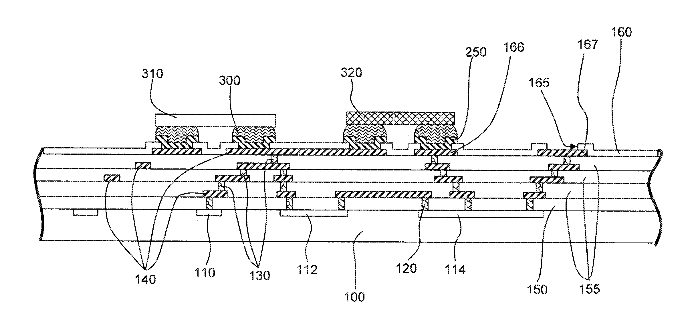
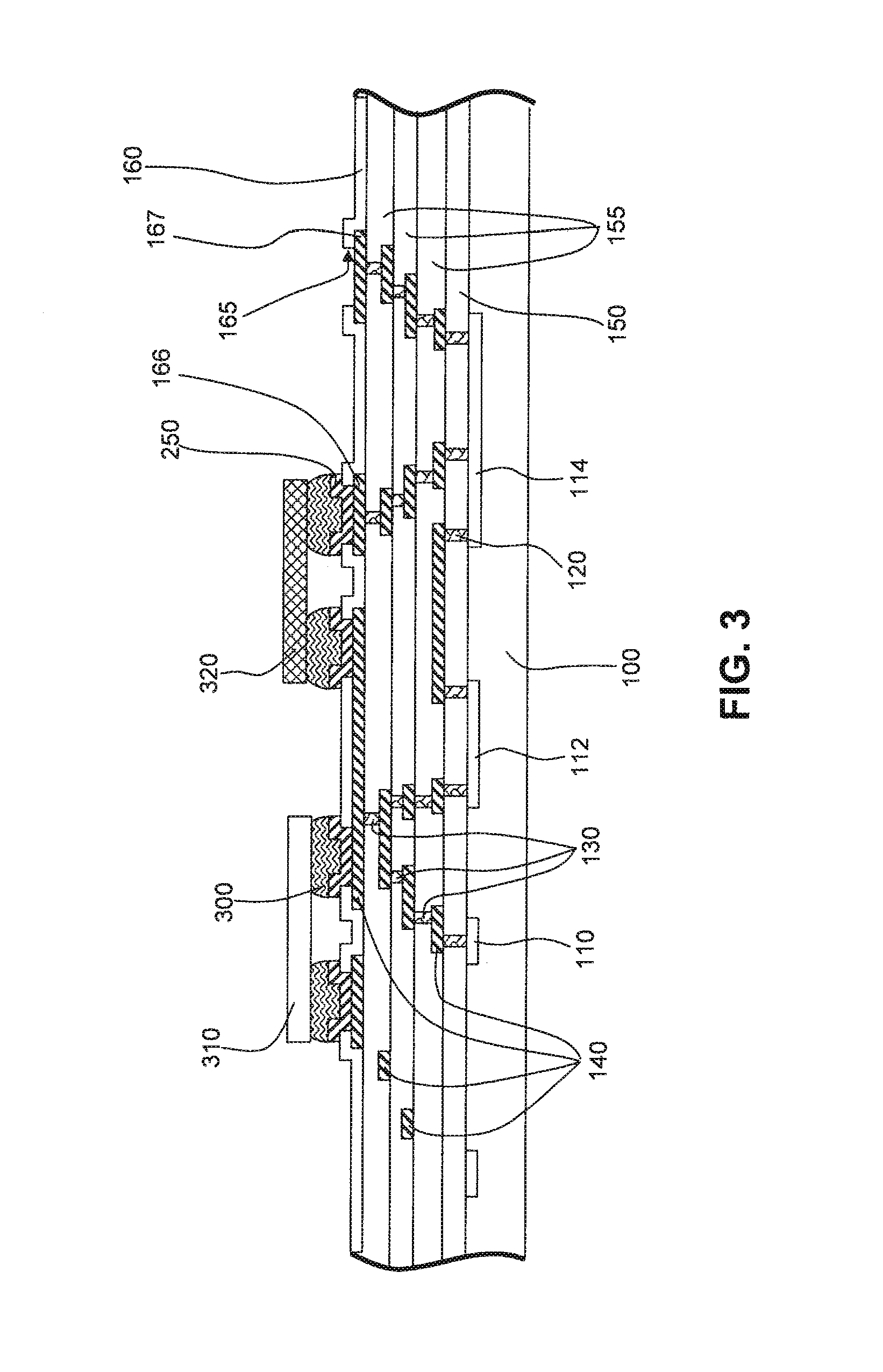
[0060]FIG. 3 depicts a substrate 100 made of a type of semiconductor base. This substrate can be silicon based, gallium arsenide (GaAs) based, silicon indium based (SiIn), silicon antimony based (SiSb), indium antimony based (InSb), or silicon germanium (SiGe) based, and many of the devices, such as devices 110, 112, and 114, are located in or over substrate 100. These devices 110, 112, and 114 can mainly be active devices, though passive devices can also be included. Active devices include voltage feedback devices, switch controller, or MOS devices, such as p-channel MOS devices, n-channel MOS devices, n-channel DMOS devices, p-channel DMOS devices, LDMOS, BiCMOS devices, Bipolar Junction Transistor (BJT), or CMOS.

[0061]As shown in FIG. 3, a thin circuit structure can be disposed or located on substrate 100. This circuit structure can include a first dielectric layer 150, multiple metal layers 140, and at least one second dielectric layer 155. The thicknesses of the first dielectri...

embodiment 2

[0085]Referring to FIG. 4, a chip structure according to a second embodiment (“Embodiment 2”) of the present disclosure is similar to that of the above-described first embodiment (“Embodiment 1”), and therefore an explanation of some of the manufacturing processes and properties will not be repeated. A difference between Embodiment 2 and Embodiment 1 lies in an under bump metal structure 260 and a bonding metal layer 400c that are constructed on or over a pad 166b. The bonding metal layer 400c can be used to connect electrically to external circuits through a copper wire or gold wire formed by wire-bonding (not shown in figure).

[0086]The structure of Embodiment 2 can be manufactured by suitable methods, including the following methods:

Manufacturing Method of Embodiment 2:

[0087]Referring to FIG. 4A, integrated circuit 20 represents all structures below passivation layer 160. Also included in integrated circuit 20 are substrate 100, devices 110, 112, 114, first dielectric layer 150, m...

embodiment 3

[0126]Referring to FIG. 5, a third embodiment (“Embodiment 3”) is shown which is similar to Embodiment 2, with a difference being the material and thickness of connecting metal layer 400. In Embodiment 3, solder layer 400 is constructed on pad 166a and 166b. The following is a description of the formation of the structure of Embodiment 3.

Manufacturing Method of Embodiment 3:

[0127]Embodiment 3 can continue from FIG. 4R of manufacturing method 2 of Embodiment 2. Referring to FIG. 5A, a solder layer 400 is formed on metal layer 44 in photoresist layer openings 40a by an electroplating method. The thickness of solder layer 400 can be selected as desired, e.g., between about 30 micrometers and about 350 micrometers. Preferred materials for solder layer 400 include fin / silver, tin / copper / silver, and tin / lead alloy.

[0128]Referring to FIG. 5B, a removal process can be applied to remove the patterned photoresist layer 40 and the portions of seed layer 38 and adhesive / barrier layer 22 that ar...


PUM


Abstract

Chip packages having power management integrated circuits are described. Power management integrated circuits can be combined with on-chip passive devices, and can provide voltage regulation, voltage conversion, dynamic voltage scaling, and battery management or charging. The on-chip passive devices can include inductors, capacitors, or resistors. Power management using a built-in voltage regulator or converter can provide for immediate adjustment of the voltage range to that which is needed. This improvement allows for easier control of electrical devices of different working voltages and decreases response time of electrical devices. Related fabrication techniques are described.

Description

CROSS-REFERENCE TO RELATED APPLICATION[0001]This application is a divisional of U.S. patent application Ser. No. 12 / 645,361, filed on Dec. 22, 2009, which claims the benefit of U.S. Provisional Application No. 61 / 140,895, filed on Dec. 26, 2008, the disclosures of which are expressly incorporated by reference herein in their entireties.BACKGROUND[0002]Conventional printed circuit boards (PCBs) typically have various components having different power inputs requiring different voltages. For a PCB with multiple electrical devices, each with potentially different voltage demands, power supplies having different output voltages are commonly used. These output voltages are typically selected to correspond to general voltage ranges that are used by the electrical devices of the PCB. Such an approach, however, consumes a rather large amount of energy, increases the difficulty of designing circuits, and also has a rather high cost. Currently, in order to accommodate many different voltage r...

Claims


Application Information

Patent Timeline
Patent Type & Authority Applications(United States)
IPC IPC(8): H01L23/532
CPCH01L23/5329H01L23/642H01L23/645H01L25/16H01L2224/16H01L2224/48091H01L2224/48247H01L2224/48465H01L2924/01013H01L2924/01029H01L2924/01046H01L2924/01077H01L2924/01078H01L2924/01079H01L2924/04941H01L2924/09701H01L2924/12044H01L2924/13091H01L2924/14H01L2924/15192H01L2924/15311H01L2924/19041H01L2924/19042H01L2924/19104H01L2924/30107H01L2924/3011H01L24/48H01L2924/01019H01L2224/16145H01L2224/16225H01L2224/32145H01L2224/32225H01L2224/48145H01L2224/48227H01L2224/73265H01L2924/15331H01L2224/16245H01L2224/45124H01L2224/45144H01L2224/45147H01L25/0652H01L2924/10253H01L24/45H01L2924/01015H01L2924/01047H01L2924/1305H01L2224/45139H01L24/73H01L2224/05027H01L2224/05569H01L2224/05008H01L2224/05022H01L2224/0508H01L2224/05568H01L2224/05023H01L2224/05001H01L2224/05572H01L2224/05124H01L2224/05139H01L2224/05144H01L2224/05147H01L2224/05155H01L2224/05164H01L2224/05166H01L2224/05171H01L2224/05181H01L2224/05184H01L2224/05624H01L2224/05639H01L2224/05644H01L2224/05647H01L2224/05655H01L2224/05664H01L2224/05666H01L2224/05684H01L2924/181H01L2224/05186H01L2924/00011H01L24/05H01L24/03H01L2224/0615H01L2924/00014H01L2924/00H01L2924/00012H01L2924/01074H01L2924/04953H01L2924/01004H01L2224/45015H01L2924/207G05F1/56H01L23/12H01L27/06
Inventor LIN, MOU-SHIUNGLEE, JIN-YUAN
Owner QUALCOMM INC
Why Eureka
Try Eureka