Nano-structure manufacturing method using sacrificial etching mask

a manufacturing method and nano-structure technology, applied in nanoinformatics, instruments, material analysis, etc., can solve the problems of contamination of compound semiconductor specimens, low surface density, and limited consistency of quantum dot specimens of low surface density, so as to reduce the number of processing steps

Inactive Publication Date: 2014-01-30
KOREA INST OF SCI & TECH
View PDF3 Cites 4 Cited by
  • Summary
  • Abstract
  • Description
  • Claims
  • Application Information

AI Technical Summary

Benefits of technology

[0013]Therefore, an inexpensive and simplified nano-structure manufacturing method which may prevent a specimen from being contaminated or damaged without using an E-beam lithography system is demanded.
[0015]According to an aspect of the present disclosure, it is possible to prevent a specimen from being contaminated by E-beam resist or damaged by E-beam, and also nano-structures may be rapidly manufactured on a large area of a specimen through reduced number of processing steps.

Problems solved by technology

However, optical devices conventionally used for measuring features of a single quantum dot do not have enough resolution to distinguish signals from the adjacent quantum dots grown with a surface density higher than 1 μm−2.
Therefore, there is a limit in consistent reproduction of quantum dot specimens of a low surface density.
The conventional mesa or micropillar manufacturing method has several disadvantages such as the complicated processing steps, the contamination of a compound semiconductor specimen due to coating of E-beam resist, the damage of a specimen due to electron collision caused by E-beam irradiation.
Moreover, expensive operation fee and slow operation speed of an E-beam lithography system severely limit manufacturing nano-structures on a large area of a specimen.

Method used


Image

  • Nano-structure manufacturing method using sacrificial etching mask
  • Nano-structure manufacturing method using sacrificial etching mask
  • Nano-structure manufacturing method using sacrificial etching mask

Examples


Embodiment Construction

[0025]Hereinafter, embodiments of the present disclosure will be described in detail with reference to the accompanying drawings.

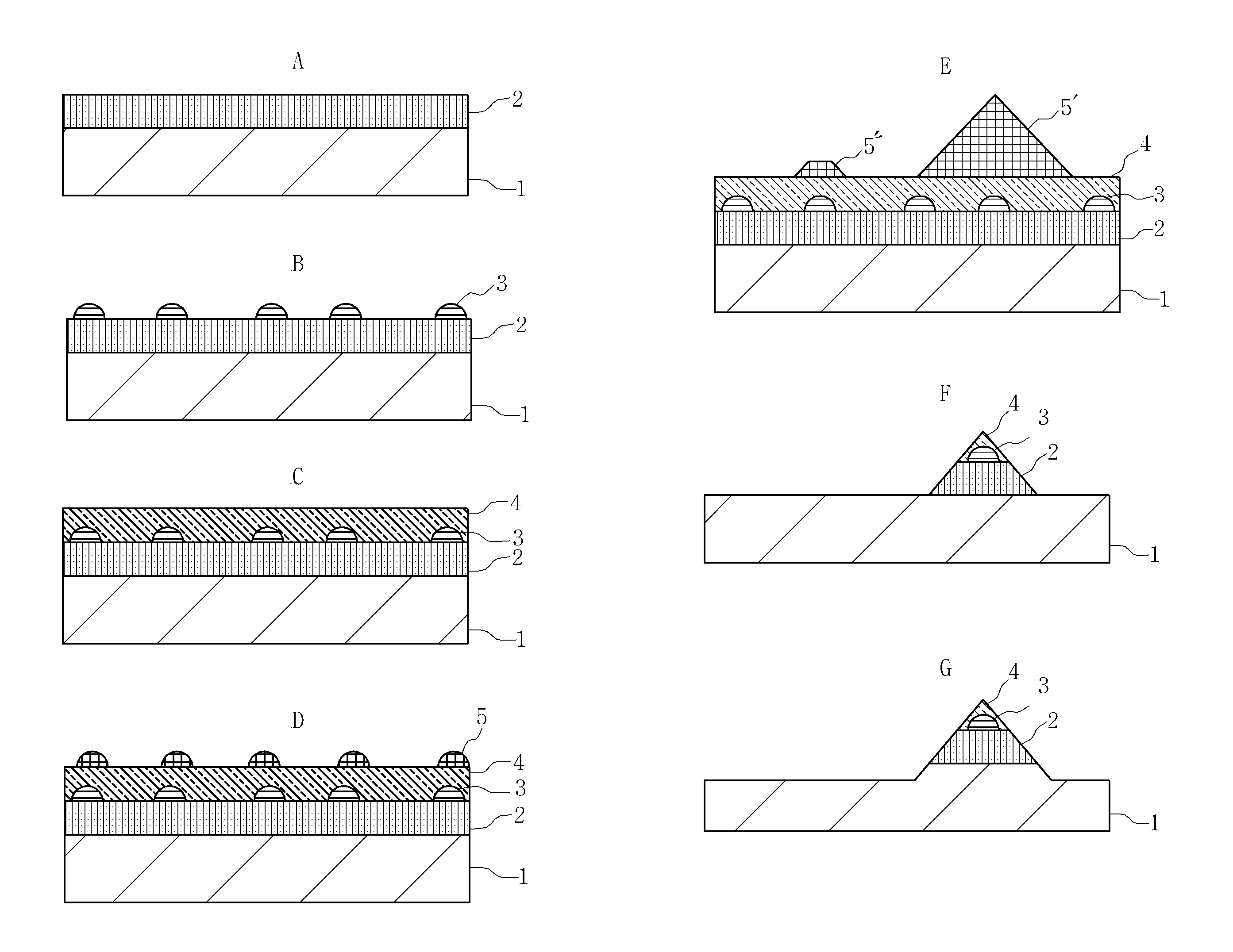
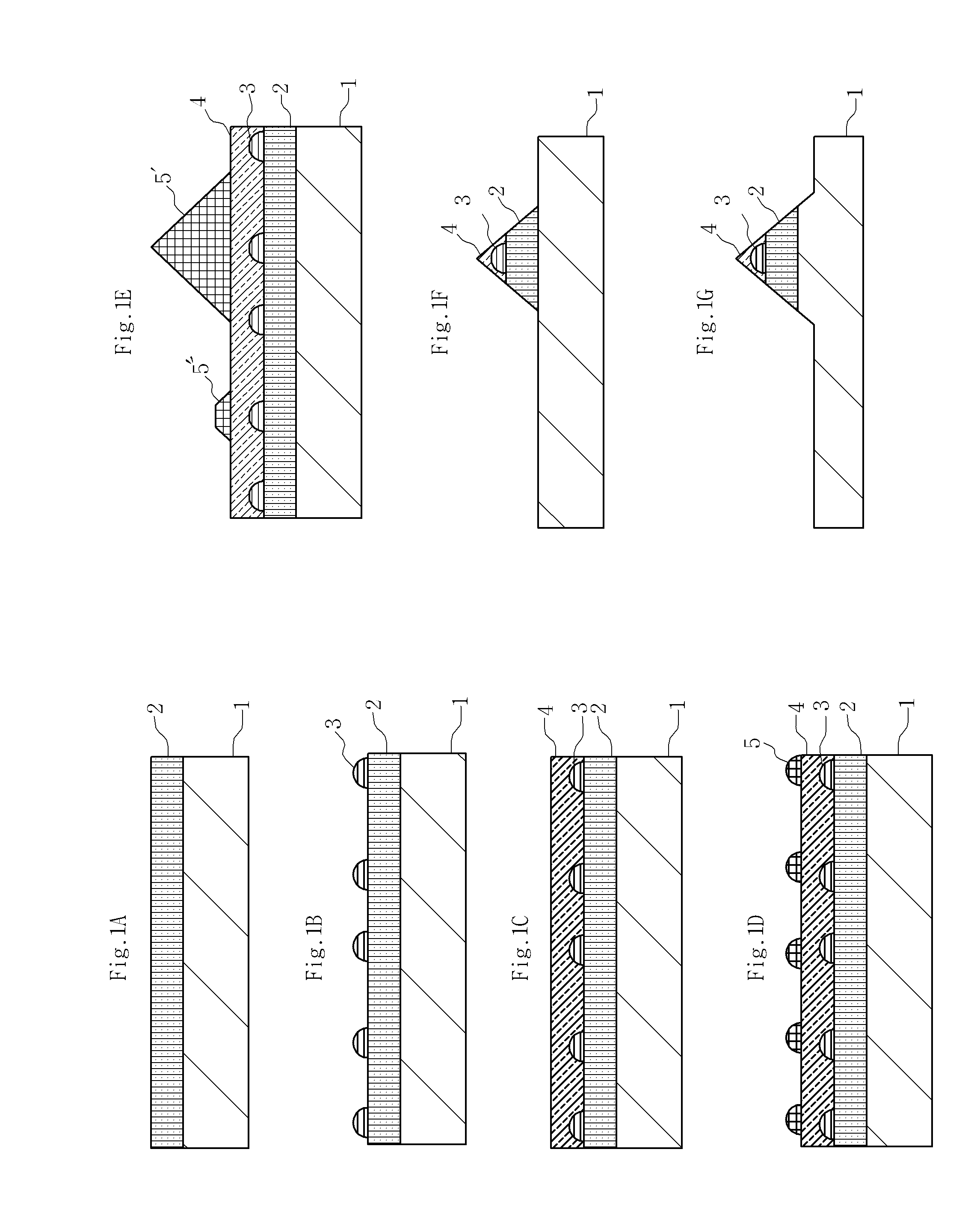
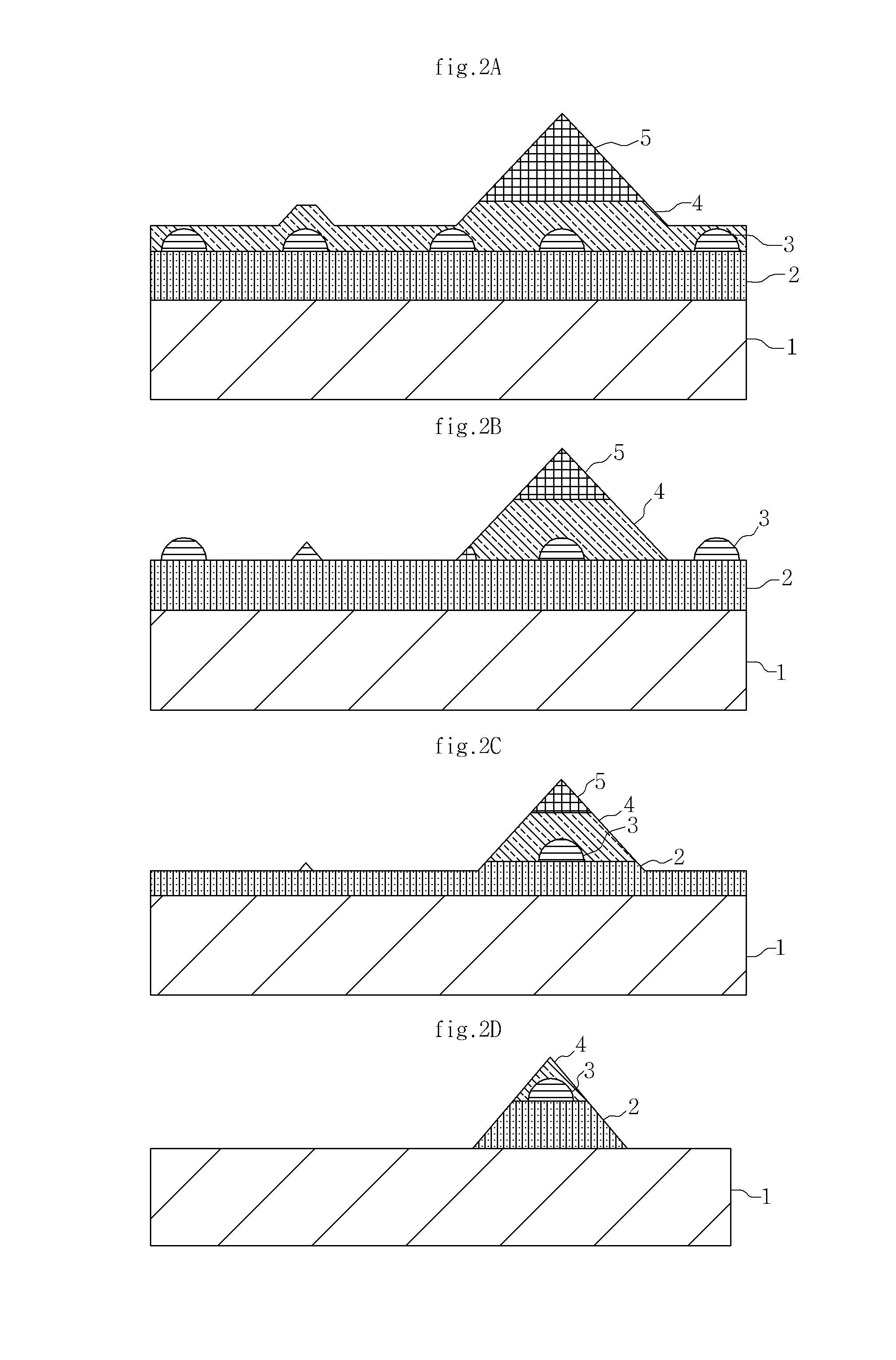
[0026]FIG. 1A-B show a nano-structure manufacturing method according to an embodiment of the present disclosure.

[0027]As shown in FIG. 1A, a first semiconductor composite layer 2 may be formed on a semiconductor substrate 1. In addition, as shown in FIG. 1B, a semiconductor quantum structure layer 3 may be formed on the first semiconductor composite layer 2. In addition, as shown in FIG. 1C, a second semiconductor composite layer 4 may be formed on the semiconductor quantum structure layer 3.

[0028]The semiconductor quantum structure layer 3 may be formed with the same material and structure as, or different material and structure from, the semiconductor quantum dot layer which operates as a sacrificial mask. In addition, the semiconductor quantum structure layer may include a quantum dot as well as various quantum structures such as a quantum wire, a quant...


PUM


Abstract

Disclosed is a nano-structure manufacturing method which includes: forming a first semiconductor composite layer, a semiconductor quantum structure layer, a second semiconductor composite layer, and a semiconductor quantum dot layer on a substrate in order; thermally treating the semiconductor quantum dot layer so that quantum dots of the semiconductor quantum dot layer are aggregated; and performing an etching process by using the aggregated quantum dots as a mask.

Description

CROSS-REFERENCE TO RELATED APPLICATION[0001]This application claims priority to Korean Patent Application No. 10-2012-0081674, filed on Jul. 26, 2012, and all the benefits accruing therefrom under 35 U.S.C. §119, the contents of which in its entirety are herein incorporated by reference.BACKGROUND[0002]1. Field[0003]The present disclosure relates to a method for manufacturing nano-structures disposed to decrease surface density of semiconductor quantum structures which have quantum confinement effect like semiconductor quantum dots, and more particularly, to a nano-structure manufacturing method using a sacrificial etching mask.[0004]2. Description of the Related Art[0005]The semiconductor material shows features different from its bulk structure when quantum confinement effect is applied by forming nano-structures like a quantum well, a quantum wire, or a quantum dot. It is because state and distribution of the electrons in the semiconductor material structure change according to t...

Claims


Application Information

Patent Timeline
Patent Type & Authority Applications(United States)
IPC IPC(8): H01L21/02
CPCB82Y40/00H01L21/02104B82Y10/00H01L21/02546H01L21/02601H01L21/02631H01L29/0665H01L29/127H01L29/7613Y10S977/84H01L21/20G01N21/00
Inventor HA, SEUNG KYUKIM, SU YOUNHAN, IL KISONG, JIN DONGCHOI, WON JUN
Owner KOREA INST OF SCI & TECH
Why Eureka
Try Eureka