

High breakdown voltage semiconductor device
a semiconductor and high-detection technology, applied in the direction of semiconductor devices, basic electric elements, electrical apparatus, etc., can solve the problems of increasing power loss, reducing the on-resistance of the mosfet, and reducing the drift resistance, so as to mutual diffusion, reduce the influence of process variation, and be easy to lay out
- Summary
- Abstract
- Description
- Claims
- Application Information
AI Technical Summary
Benefits of technology
Problems solved by technology
Method used
Image

Examples
first embodiment
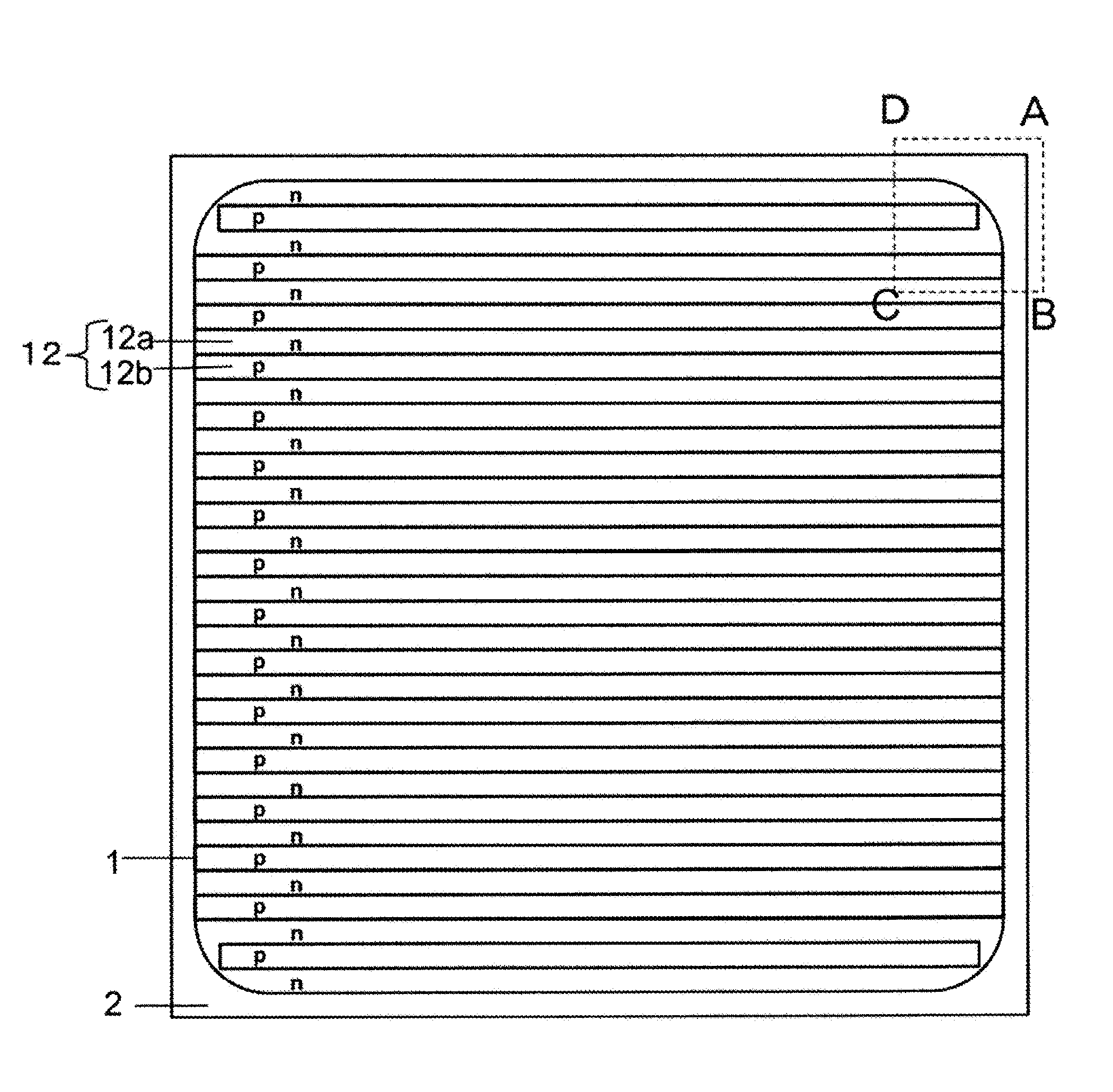
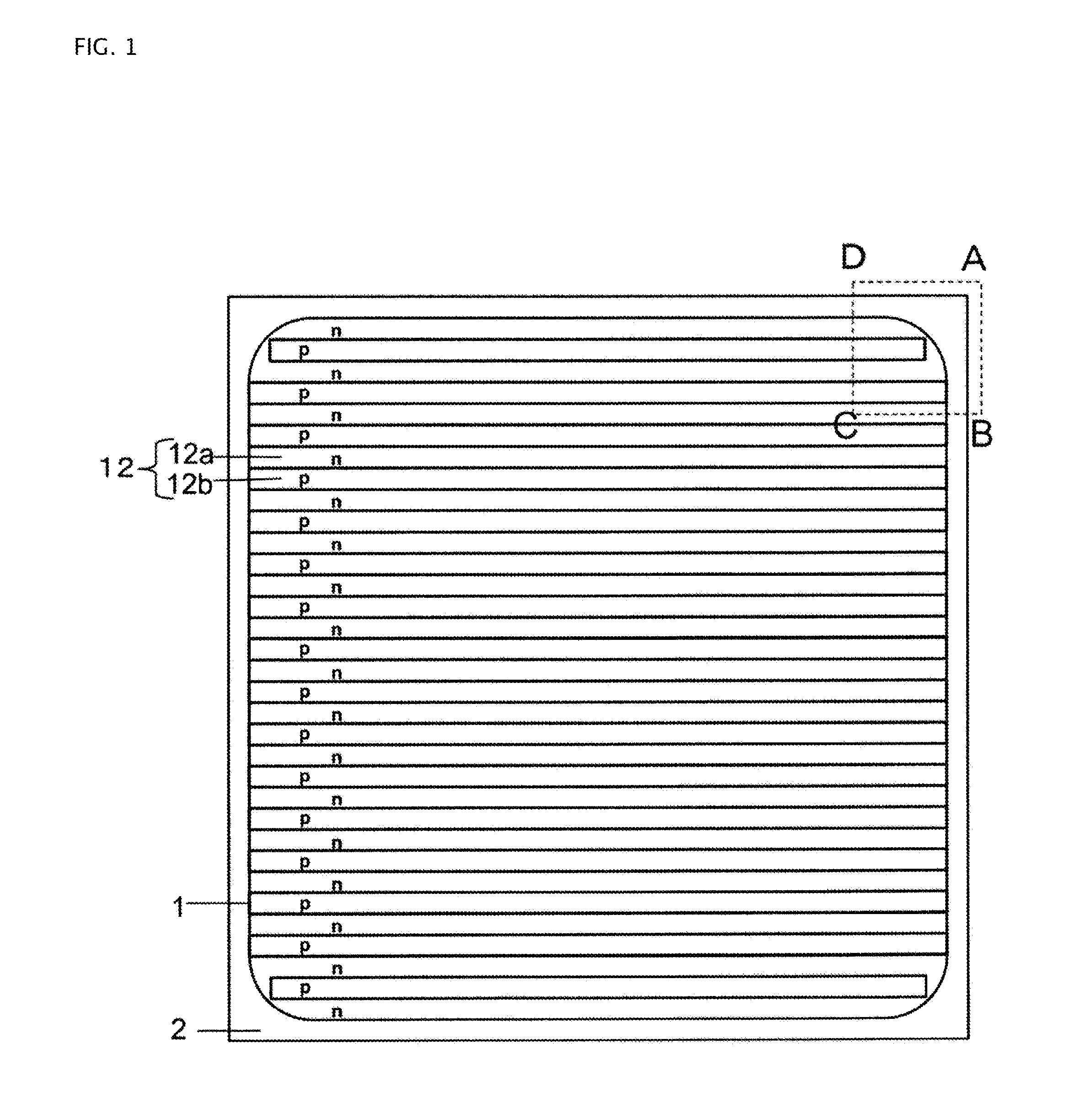
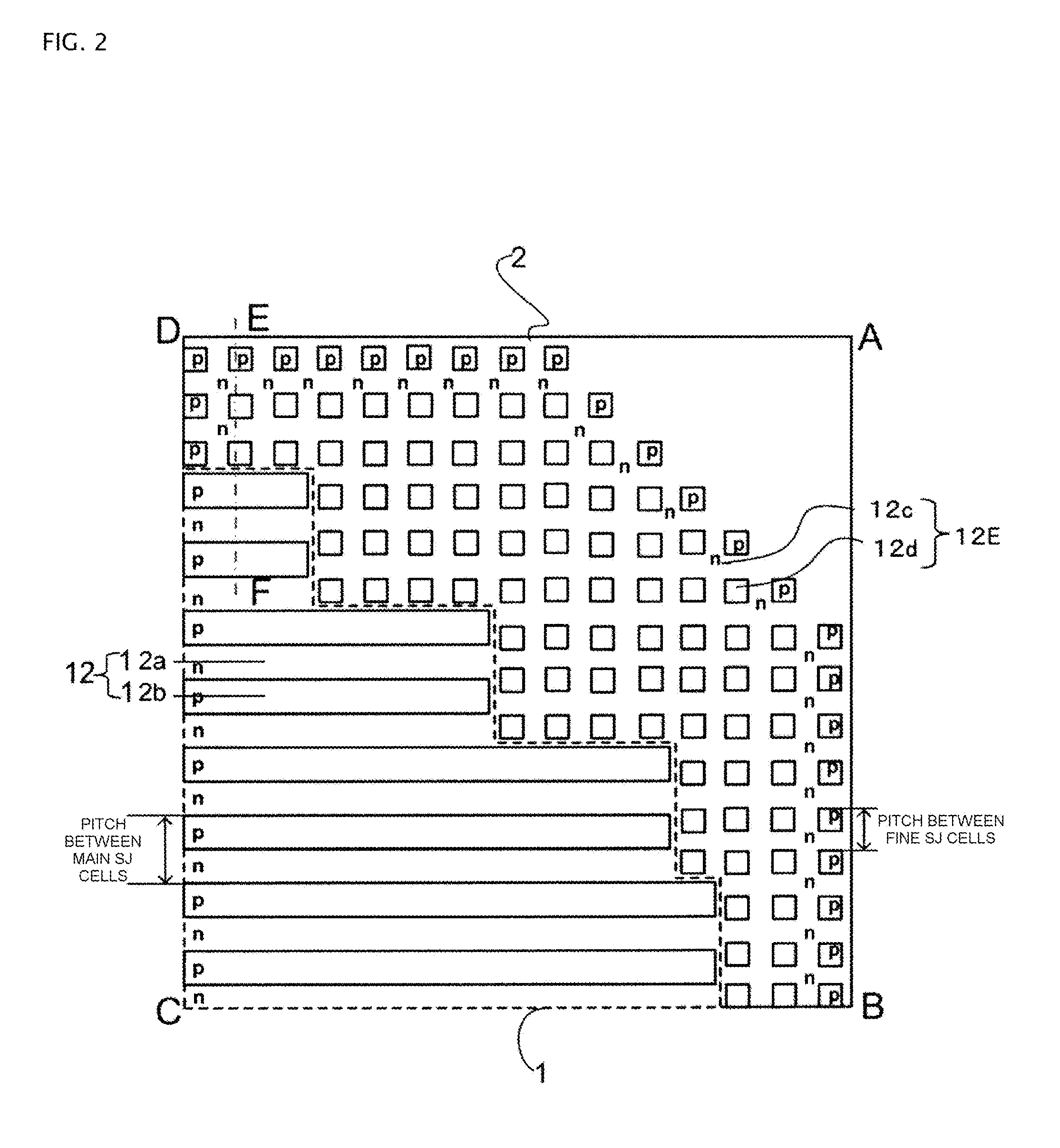
[0031]As an example of a high breakdown voltage semiconductor device according to a first embodiment, a vertical MOSFET (hereinafter, referred to as an SJ-MOSFET) with a superjunction (SJ) structure will be described. FIG. 1 is a plan view illustrating the structure of the SJ-MOSFET according to the first embodiment of the invention. FIG. 2 is an enlarged plan view illustrating a portion surrounded by a rectangle having vertexes A, B, C, and D in FIG. 1. FIGS. 1 and 2 illustrate only the planar layout of the SJ structure in order to clarify the planar structure of the SJ structure.
[0032]As illustrated in FIGS. 1 and 2, in the SJ-MOSFET according to the first embodiment of the invention, main SJ cells are provided in a drift layer in active region 1 and fine SJ cells are provided in the drift layer in edge termination region 2. Active region 1 is a region which serves as a current path when the device is turned on. Edge termination region 2 is a region which reduces the electrical fi...
second embodiment
[0049]FIG. 5 is an enlarged plan view illustrating a portion of an SJ-MOSFET according to a second embodiment of the invention. FIG. 6 is a cross-sectional view illustrating a cross-sectional structure along the cutting line G-H of FIG. 5. FIG. 5 illustrates another example of the portion surrounded by the rectangle ABCD in FIG. 1. There are two differences between the SJ-MOSFET according to the second embodiment and the SJ-MOSFET according to the first embodiment. The first difference is that the parallel pn layers (main SJ cell 12) which are arranged in a repetitive pattern in active region 1 do not have a stripe-shaped planar layout, but have a planar layout in which p partition regions 12b are arranged in a matrix in n drift region 12a.
[0050]The second difference is that n− region 3 is not formed as a uniform impurity concentration region in the surface of edge termination region 2. The SJ-MOSFET according to the second embodiment has the same structure as the SJ-MOSFET accordi...
PUM
 Abstract
Description
Claims
Application Information