Thin film transistor and manufacturing method therefor, and display device

a manufacturing method and technology applied in the field manufacturing methods therefor, can solve the problems of increasing the cost of i-line exposure devices, and increasing the cost of large-type i-line exposure devices. achieve the effect of reducing the oxide semiconductor layer, increasing the current driving force of thin film transistors, and increasing the number of transistors

Active Publication Date: 2014-02-06
SHARP KK
View PDF3 Cites 48 Cited by
  • Summary
  • Abstract
  • Description
  • Claims
  • Application Information

AI Technical Summary

Benefits of technology

[0052]According to the first aspect, because the resistance value of the second region sandwiched between the two first regions that are formed in the channel layer is higher than the resistance values of the first regions, the second region functions as the channel of the thin film transistor. In accordance with the forming of the first regions, the length of the second region can be made shorter than the length between the end part of the source electrode and the end part of the drain electrode that is determined by the resolution limit of the exposure device. Accordingly, because the electrical channel length becomes short, the current driving force of the thin film transistor becomes large.
[0053]According to the second aspect, by applying a voltage to the gate electrode, the length of the second region becomes long by the shortened length of the first regions. Because the length of the second region becomes shorter than the length between the end part of the source electrode and the end part of the drain electrode, the current driving force can be made larger than that of the conventional thin film transistor.
[0054]According to the third aspect, the metal electrodes take oxygen away from the oxide semiconductor layer, and at the same time, supply hydrogen to the oxide semiconductor layer. The oxide semiconductor layer is reduced, hydrogen is spread inside this layer, and the first regions having low resistance values are formed in the oxide semiconductor layer. Accordingly, because the electrical channel length becomes short, the current driving force of the thin film transistor can be made large.
[0055]According to the fourth aspect, also in the thin film transistor of the channel etch structure, the electrical channel length is shortened by forming the first regions. Accordingly, the current driving force of the thin film transistor of the channel etch structure can be made large.
[0056]According to the fifth aspect, also in the thin film transistor of the etch stopper structure, the electrical channel length is shortened by forming the first regions. Accordingly, the current driving force of the thin film transistor of the etch stopper structure can be made large.
[0057]According to the sixth aspect, also in the thin film transistor of the bottom contact structure, the electrical channel length is shortened by forming the first regions. Accordingly, the current driving force of the thin film transistor of the bottom contact structure can be made large.

Problems solved by technology

However, the i-line exposure device is more expensive than the g-line+h-line exposure device, and a large-type i-line exposure device that can expose a large-type substrate becomes more expensive.

Method used


Image

  • Thin film transistor and manufacturing method therefor, and display device
  • Thin film transistor and manufacturing method therefor, and display device
  • Thin film transistor and manufacturing method therefor, and display device

Examples


first embodiment

2. First Embodiment

2.1 Configuration of TFT

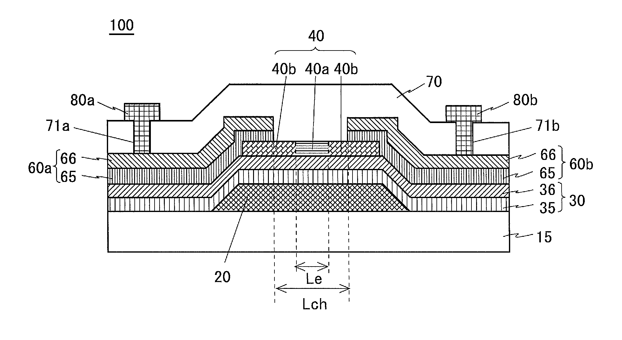
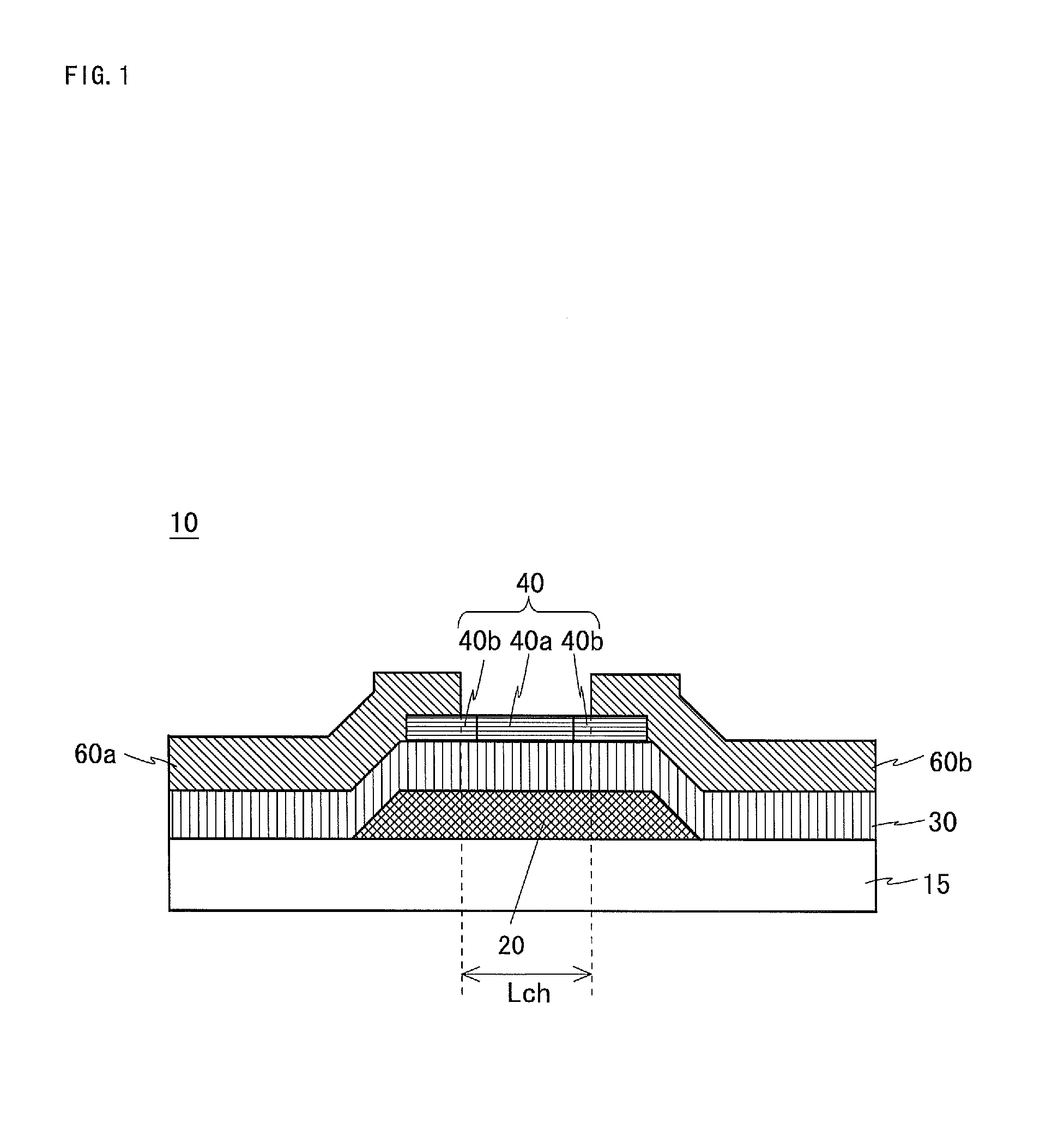
[0112]FIG. 7(a) is a plan view showing a configuration of a bottom-gate type TFT 100 according to a first embodiment of the present invention, and FIG. 7(b) is a cross-sectional view along the A-A line shown in FIG. 7(a). The TFT 100 shown in FIG. 7(a) and FIG. 7(b) are also referred to as a TFT of a channel etch structure. The configuration of the TFT 100 is described with reference to FIG. 7(a) and FIG. 7(b).

[0113]The gate electrode 20 is formed on the insulating substrate 15 such as a glass substrate. The gate electrode 20 is configured by a laminated metal film obtained by laminating a copper (Cu) film on a titanium film, for example. The gate electrode 20 may be configured by a laminated metal film obtained by laminating a titanium film, an aluminum (Al) film, and a titanium film in order from the insulating substrate 15 side.

[0114]The gate insulating film 30 is formed to cover the whole surface of the insulating substrate 15 including...

second embodiment

3. Second Embodiment

3.1 Configuration of TFT

[0156]FIG. 14(a) is a plan view showing a configuration of a bottom-gate type TFT 200 according to the second embodiment of the present invention, and FIG. 14(b) is a cross-sectional view along the B-B line of the TFT 200 shown in FIG. 14(a). The TFT 200 shown in FIG. 14(a) and FIG. 14(b) is also referred to as a TFT of an etch stopper structure.

[0157]The configuration of the TFT 200 is described with reference to FIG. 14(a) and FIG. 14(b). On the insulating substrate 15 such as a glass substrate, the gate electrode 20 is formed. To cover the whole surface of the insulating substrate 15 including the gate electrode 20, the gate insulating film 30 is formed. Because the configurations of the gate electrode 20 and the gate insulating film 30 are the same as those of the TFT 100 according to the first embodiment, the same reference marks are attached and their descriptions are omitted.

[0158]On the surface of the gate insulating film 30 at a p...

third embodiment

4. Third Embodiment

4.1 Configuration of TFT

[0177]FIG. 18(a) is a plan view showing a configuration of a bottom-gate type TFT 300 according to a third embodiment of the present invention, and FIG. 18(b) is a cross-sectional view along the C-C line of the TFT 300 shown in FIG. 18(a). The TFT 300 shown in FIG. 18(a) and FIG. 18(b) is also referred to as a TFT of a bottom contact structure.

[0178]The configuration of the TFT 300 is described with reference to FIG. 18(a) and FIG. 18(b). On the insulating substrate 15, the gate electrode 20 is formed. To cover the whole surface of the insulating substrate 15 including the gate electrode 20, the gate insulating film 30 is formed. Because the configurations of the gate electrode 20 and the gate insulating film 30 are the same as those in the TFT 100 according to the first embodiment, the same reference marks are attached, and their descriptions are omitted.

[0179]On the gate insulating film 30 above the gate electrode 20, a source electrode 2...


PUM


Abstract

The invention provides a thin film transistor having current driving force that can be substantially improved. By heat treatment, the IGZO layer (45) from which oxygen is taken away by the titanium electrodes (65) becomes the low resistance regions (40b), and the IGZO layer (45) from which oxygen is not taken away remains as the high resistance region (40a). In this state, when the gate voltage is applied to the gate electrode (20), electrons in the low resistance regions (40b) near the boundaries with the high resistance region (40a) move respectively to the titanium electrode (65) sides. As a result, the length of the low resistance regions (40b) becomes short, and oppositely, the length of the high resistance region (40a) becomes longer by the size of the shortened low resistance regions. However, the electrical channel length (Le) becomes shorter than the source/drain interval space (Lch) as the limit resolution of the exposure device, and the current driving force becomes large.

Description

TECHNICAL FIELD[0001]The present invention relates to a thin film transistor and a manufacturing method therefor, and a display device, and particularly relates to a thin film transistor having a channel layer made of an oxide semiconductor and a manufacturing method therefor, and a display device.BACKGROUND ART[0002]In recent years, by focusing attention to the excellent characteristic of an oxide semiconductor made of indium gallium zinc oxide (hereinafter, referred to as “IGZO”) and the like, there has been progressed the development of a thin film transistor (hereinafter, referred to as “TFT”) that has the oxide semiconductor as a channel layer.[0003]To increase the current driving force of a TFT, it is most effective to shorten the channel length. The channel length is equivalent to the length between the end part of the source electrode and the end part of the drain electrode, and this length is determined by a resolution limit of the exposure device. The resolution limit is d...

Claims


Application Information

Patent Timeline
Patent Type & Authority Applications(United States)
IPC IPC(8): H01L29/786H05B37/02H01L29/66
CPCH01L29/7869H05B37/02H01L29/66742H01L29/45H01L29/66969H01L29/78618G02F1/1368H01L27/1225H01L29/41733H01L29/4908H01L29/78696H05B47/10
Inventor KITAKADO, HIDEHITOKATOH, SUMIO
Owner SHARP KK
Why Eureka
Try Eureka