Semiconductor Device And Method For Producing Light And Laser Emission

a semiconductor and laser technology, applied in semiconductor lasers, laser details, electrical apparatus, etc., can solve the problems of limited current injection into the cascade region, two terminal n+-i-n semiconductor devices, and the greater challenge of direct modulation at high speed for qcl lasers, so as to reduce free-carrier absorption, reduce power external rf drive circuitry, and facilitate switching or modulation

Active Publication Date: 2014-02-20
THE BOARD OF TRUSTEES OF THE UNIV OF ILLINOIS
View PDF3 Cites 12 Cited by
  • Summary
  • Abstract
  • Description
  • Claims
  • Application Information

AI Technical Summary

Benefits of technology

[0025]A representation of the family of curves for a BJT under standard operation is illustrated in FIG. 6. As seen in the Figure, collector current is controlled by the base current Ib, and is largely independent of collector-emitter voltage. Collector current is related to the base current by the amplification factor β, which is a characteristic of the device determined by design. The collector current Ic can be easily switched or modulated with the smaller base current Ib. Additionally, since the magnitude of the current flowing through the base-collector junction is largely independent of base-collector reverse bias voltage and determined almost exclusively by the emitter-base current, currents can be switched through the base-collector junction with minimal change to the electric field in that junction.
[0026]In accordance with a feature of embodiments of the invention, an HBT-like device architecture is utilized to control current injection into a QCL type of structure (i.e., the cascade region thereof) located in the field region of the base-collector junction of a transistor device. This approach decouples field from current in the cascade region, allowing independent control of both parameters. This has fundamental advantages over an n+-i-n structure where field and current cannot be decoupled. There is a clear advantage for modulation. The voltage drop across the forward-biased emitter-base junction is small, and switching and modulation of the large collector current IC with the much smaller base current IB allows the use of lower power external RF drive circuitry. Additionally, the field across the cascade region structure in the device remains effectively constant during modulation, so the energy levels and wave function overlap of the quantum states in the cascade region are not perturbed by the modulation voltage. From a laser perspective, where stimulated emission relies on a transition of specific energy, not changing the transition energy is advantageous. At the same time, fields in the cascade region can be controlled independently from the current flow through the region if desired. Intentionally modulating the base-collector voltage allows bi-directional wavelength mod

Problems solved by technology

At the same time, a weakness of the QCL is that it is a two terminal n+-i-n semiconductor device with current injection into the cascade region limited by the resistance of the structure and the applied voltage.
Direct modulation at high speed is therefore a greater challenge for QCL lasers.
These I-V characteristics

Method used


Image

  • Semiconductor Device And Method For Producing Light And Laser Emission
  • Semiconductor Device And Method For Producing Light And Laser Emission
  • Semiconductor Device And Method For Producing Light And Laser Emission

Examples


Embodiment Construction

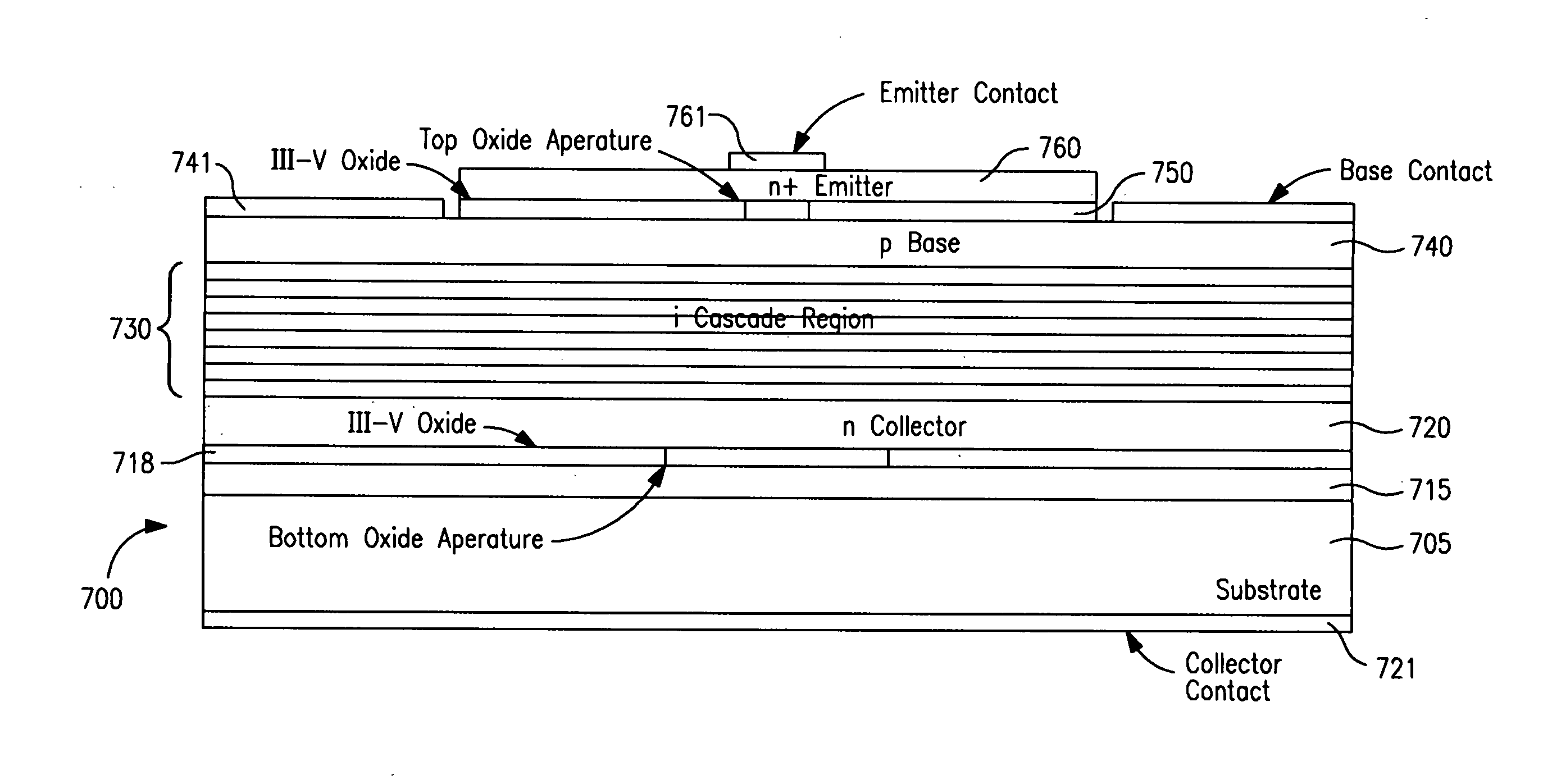
[0040]FIG. 7 is a diagram of a device 700 in accordance with an embodiment of the invention, and which can be used in practicing an embodiment of the method of the invention. Devices hereof can be made using, for example, epitaxial deposition, such as metal organic chemical vapor deposition, and molecular beam epitaxy for superlattice layers, and / or any other suitable techniques, including techniques conventionally used to fabricate heterojunction bipolar transistors (HBTs) and quantum cascade lasers (QCLs). The device of FIG. 7 employs a conductive substrate 705 having a subcollector layer 715 disposed thereon, followed by an oxide-defined aperture layer 718 and a collector layer 720 which, in the present embodiment, is n-type. The aperture can be made using a buried oxide layer, formed using lateral oxidation (see, for example, S. A. Maranowski, A. R. Sugg, E. I Chen, and N. Holonyak, Jr., “Native Oxide Top-and Bottom-Confined Narrow Stripe p-n Aly Ga1-yAs—GaAs—InxGa1-xAs Quantum ...


PUM


Abstract

A method for producing light emission, including the following steps: providing a transistor structure that includes a semiconductor base region disposed between a semiconductor emitter region and a semiconductor collector region; providing a cascade region between the base region and the collector region, the cascade region having a plurality of sequences of quantum size regions, the quantum size regions of the sequences varying, in the direction toward the collector region, from a relatively higher energy state to a relatively lower energy state; providing emitter, base and collector electrodes respectively coupled with the emitter, base, and collector regions; and applying electrical signals with respect to the emitter, base, and collector electrodes to cause and control light emission from the cascade region.

Description

PRIORITY CLAIM[0001]Priority is claimed from U.S. Provisional Patent Application No. 61 / 742,835, filed Aug. 20, 2012, and said U.S. Provisional Patent Application is incorporated herein by reference.FIELD OF THE INVENTION[0002]This invention relates to the field of semiconductor light emitting and lasing devices and methods.BACKGROUND OF THE INVENTION[0003]Quantum cascade lasers (QCLs) are semiconductor lasers that emit in the infrared portion of the electromagnetic spectrum and were first demonstrated during the mid-1990's. Unlike typical interband semiconductor lasers that emit electromagnetic radiation through the recombination of electron-hole pairs across the material band gap, QCLs are unipolar and laser emission is achieved through the use of intersubband transitions in a superlattice.[0004]QLCs are important because of their ability to produce coherent radiation in the near to mid-IR through the terahertz frequency bands. At the same time, a weakness of the QCL is that it is...

Claims


Application Information

Patent Timeline
IPC IPC(8): H01S5/34
CPCH01S5/3401H01S5/06203H01S5/06206H01S5/2215H01S5/3419H01S5/34313H01S5/0208B82Y20/00
Inventor DALLESASSE, JOHNFENG, MILTON
Owner THE BOARD OF TRUSTEES OF THE UNIV OF ILLINOIS
Why Eureka
Try Eureka