

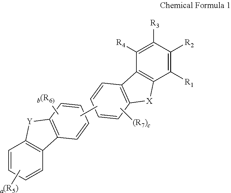
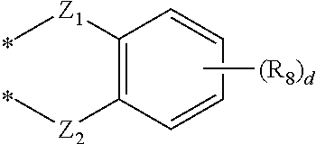
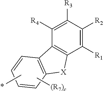
Novel compound for organic electronic material and organic electroluminescent device using the same
- Summary
- Abstract
- Description
- Claims
- Application Information
AI Technical Summary
Benefits of technology
Problems solved by technology
Method used
Image

Examples
preparation example 1
Preparation of Compound 1
[0031]
Preparation of Compound 1-1
[0032]Cyclohexane-1,2-dione 25 g (0.22 mol) was put into a 1 L 2-neck round-bottom flask, and phenylhydrazine 70.9 g (0.49 mol), H2SO4 1.18 mL (0.02 mol), and MeOH 720 mL (0.3M) were added thereinto, followed by heating to 100° C. Upon completion of the reaction after stirring for 4 hours, the resultant material was cooled down, and the thus generated solid was filtered and then washed with MeOH. The washed solid was put into a 1 L 2-neck round-bottom flask, and TFA (trifluoroacetic acid) 60 g and AcOH 600 mL were put thereinto, followed by heating and stirring at 100° C. for 12 hours. Upon completion of the reaction, washing with distilled water and then extraction with ethyl acetate were performed. The organic layer was dried over MgSO4 and the solvent was removed by a rotary evaporator, followed by purification using column chromatography, thereby obtaining Compound 1-1 17 g (29%).
Preparation of Compound 1-2
[0033]Compound ...
preparation example 2
Preparation of Compound 2
[0040]
Preparation of Compound 2-1
[0041]1-bromo-2-nitrobenzene 15 g (0.074 mol) was put into a 1 L 2-neck round bottom flask, and then 9,9-dimethyl-9H-fluoren-2-ylboronic acid 23 g (0.096 mol), Pd(PPh3)4 4.2 g (0.003 mol), Na2CO3 (2M) 111 mL, and ethanol 111 mL were put thereinto. Then, toluene 200 mL was added thereinto, followed by heating and stirring at 120° C. for 3 hours. Upon completion of the reaction, washing with distilled water and then extraction with ethyl acetate were performed. The organic layer was dried over MgSO4 and the solvent was removed by a rotary evaporator, followed by purification using column chromatography, thereby obtaining Compound 2-1 22 g (95%).
Preparation of Compound 2-2
[0042]Compound 2-1 24 g (0.076 mol) was put into a 1 L 2-neck round bottom flask, then triethylphosphite 200 mL and 1,2-dichlorobenzene 200 mL were added thereinto, followed by heating and stirring at 140° C. for 12 hours. Upon completion of the reaction, the s...
preparation example 3
Preparation of Compound 3
[0050]
Preparation of Compound 3-1
[0051]1-bromo-2-nitrobenzene 15 g (0.074 mol) was put into a 1 L 2-neck round-bottom flask, and then, the same method as the preparation of Compound 2-1 by using 5,5-dimethyl-5H-dibenzo[b,d]silol-3-ylboronic acid 24.4 g (0.096 mol), thereby obtaining Compound 3-1 22.6 g (95%).
Preparation of Compound 3-2
[0052]Compound 3-1 22.6 g (0.068 mol) was put into a 1 L 2-neck round-bottom flask, and then, the same method as the preparation of Compound 2-2 was conducted by using Compound 2-2, thereby obtaining Compound 3-2 7 g (35%).
Preparation of Compound 3-3
[0053]Compound 3-2 8.4 g (0.028 mol) was put into a 1 L 2-neck round-bottom flask, and then, the same method as the preparation of Compound 2-3 was conducted by using Compound 2-3, thereby obtaining Compound 3-3 9.1 g (86%).
Preparation of Compound 3-4
[0054]The same method as the preparation of Compound 2-4 was conducted by using Compound 3-3 9 g (0.024 mol) in a 3 L 2-neck round-bot...
PUM
 Abstract
Description
Claims
Application Information