

Organic electronic device and method for manufacturing the same
- Summary
- Abstract
- Description
- Claims
- Application Information
AI Technical Summary
Benefits of technology
Problems solved by technology
Method used
Image

Examples
examples
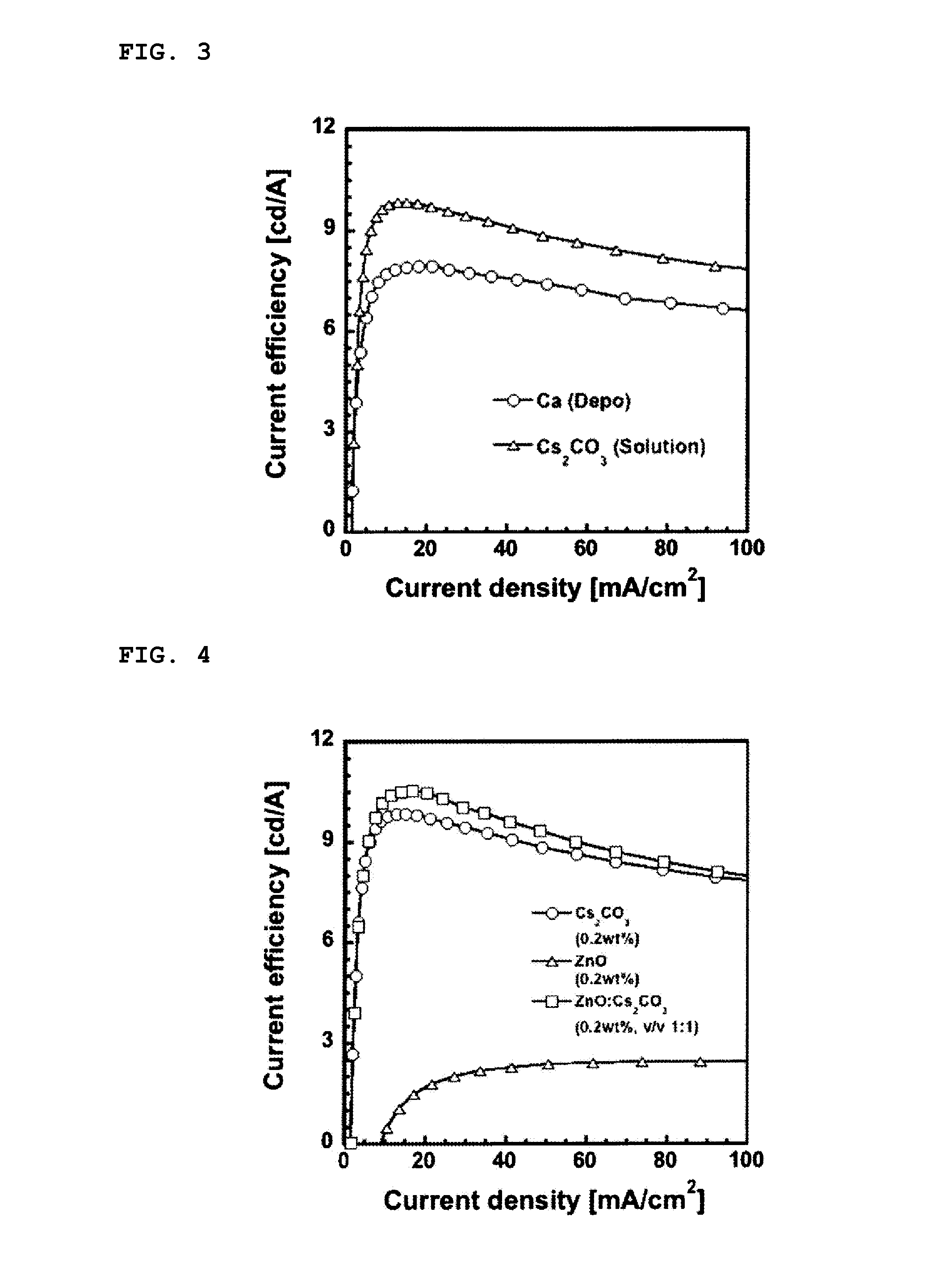
[0076]Hereinafter, the present invention will be described more particularly with reference to Examples. In the following, an organic EL element and an electron injection layer of organic electronic devices are illustrated, however, the present invention is not limited thereto.
[0077](Sample 1) Deposition Method Ca
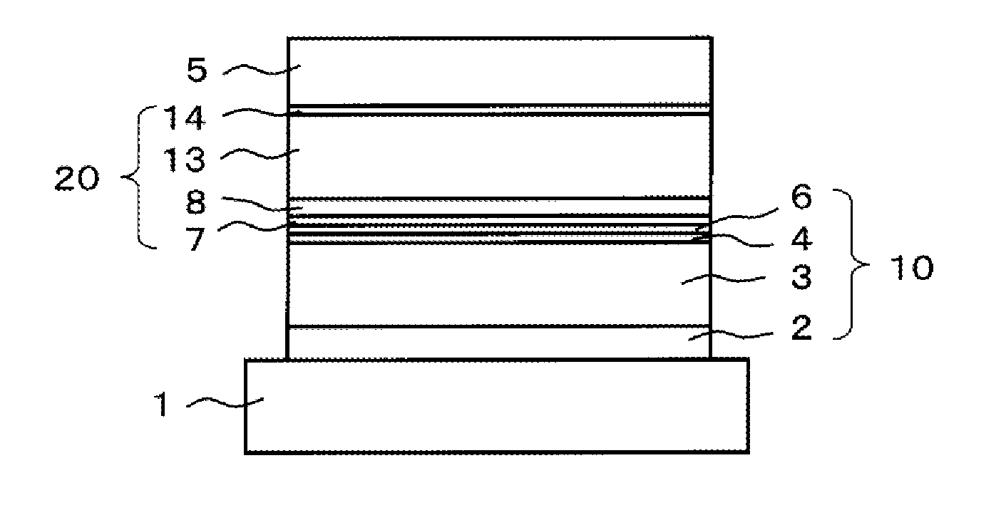
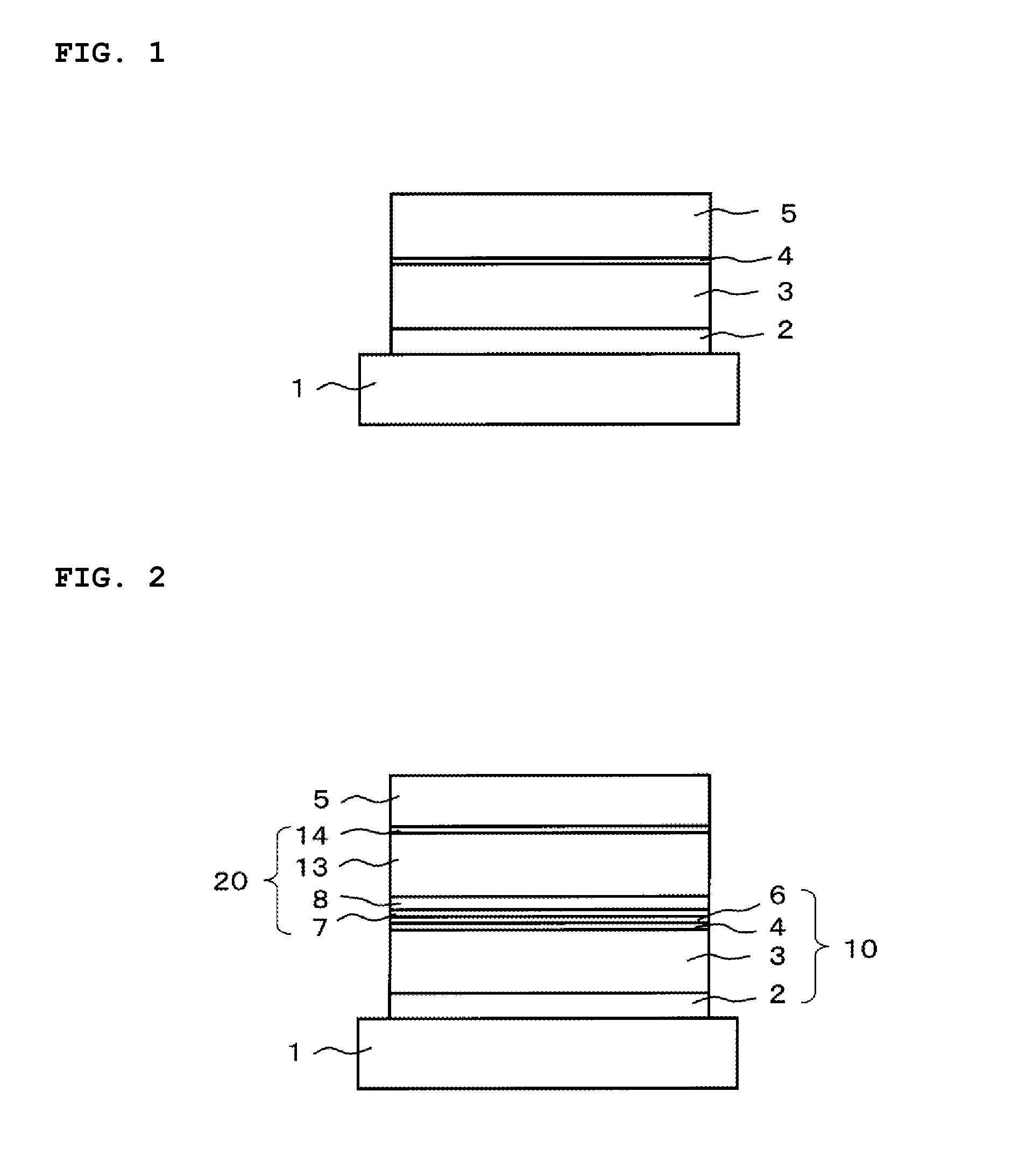
[0078]An organic EL element having a layer structure as shown in FIG. 1 was prepared where Ca formed as a film by a deposition method was used as an electron injection layer.
[0079]First, a patterned ITO substrate 1 (thickness of ITO film: 110 nm, element area: 10×10 mm2, luminescence area: 2×2 mm2) was subjected to in order of acetone ultrasonic wave washing for 20 minutes, scrub by alkali detergent, alkali detergent ultrasonic wave washing for 20 minutes, acetone ultrasonic wave washing for 20 minutes, isopropyl alcohol (IPA) ultrasonic wave washing for 20 minutes, and UV ozone washing for 20 minutes.
[0080]On the thus washed ITO substrate, five drops of PEDOT:PSS were drop...
PUM
| Property | Measurement | Unit |
|---|---|---|
| Thickness | aaaaa | aaaaa |
| Volume | aaaaa | aaaaa |
| Fraction | aaaaa | aaaaa |
Abstract
Description
Claims
Application Information