High-concentration multi-junction solar cell and method for fabricating same

a solar cell, multi-junction technology, applied in the field of compound semiconductor solar cells, can solve the problems of affecting the cell fill factor, and reducing the conversion efficiency, so as to increase the photoelectric conversion efficiency of the cell, reduce the fill factor of the cell, and increase the series resistance

Inactive Publication Date: 2014-04-03
XIAMEN SANAN OPTOELECTRONICS TECH CO LTD
View PDF5 Cites 13 Cited by
  • Summary
  • Abstract
  • Description
  • Claims
  • Application Information

AI Technical Summary

Benefits of technology

[0018]Each sub-cell emitter layer of the traditional multi-junction solar cell is uniformly doped, and the thinner the emitter layer is, the higher the photoelectric conversion efficiency of the cell is. However, under the high-concentration condition, the thinner top cell emitter layer produces greater series resistance, which decreases the fill factor of the cell and finally affects the conversion efficiency. The invention relates to a high-concentration multi-junction solar cell. The emitter layers of the top and intermediate cells both employ the graded doping concentration and have high open circuit voltage and short circuit current; meanwhile, under the high concentration condition, the top cell emitter layer is allowed to have greater thickness compared with the traditional multi-junction cell so as to decrease the total series resistance of the multi-junction cell, improve the fill factor and finally gain higher photoelectric conversion efficiency.

Problems solved by technology

Along with the comparatively high open circuit voltage and short-circuit current under high concentration (−1000×), the cell can also produce greater series resistance, which seriously affects the fill factor of cell and decreases the conversion efficiency.
However, under the high-concentration condition, the thinner top cell emitter layer produces greater series resistance, which decreases the fill factor of the cell and finally affects the conversion efficiency.

Method used


Image

  • High-concentration multi-junction solar cell and method for fabricating same
  • High-concentration multi-junction solar cell and method for fabricating same

Examples


embodiment one

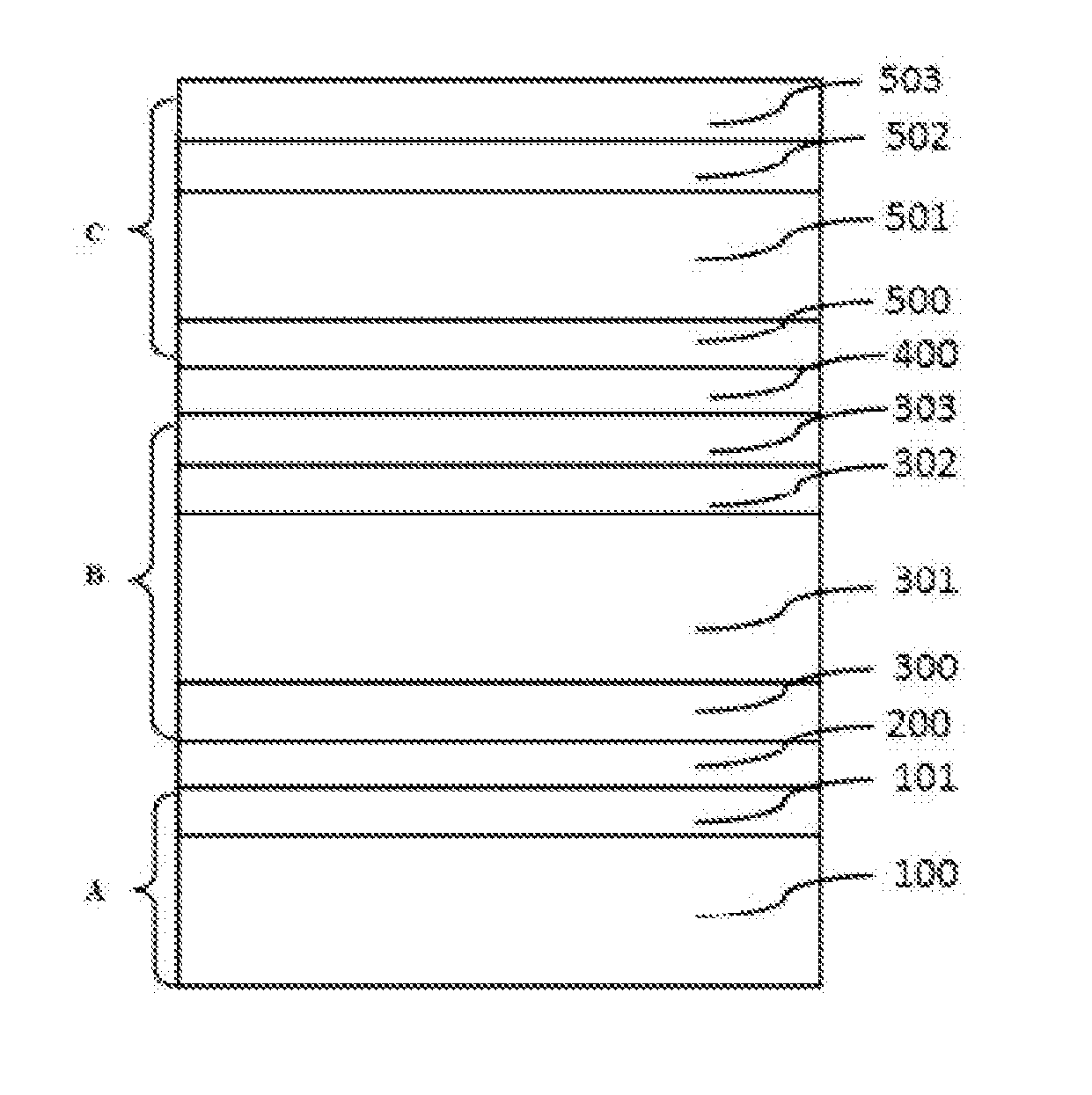
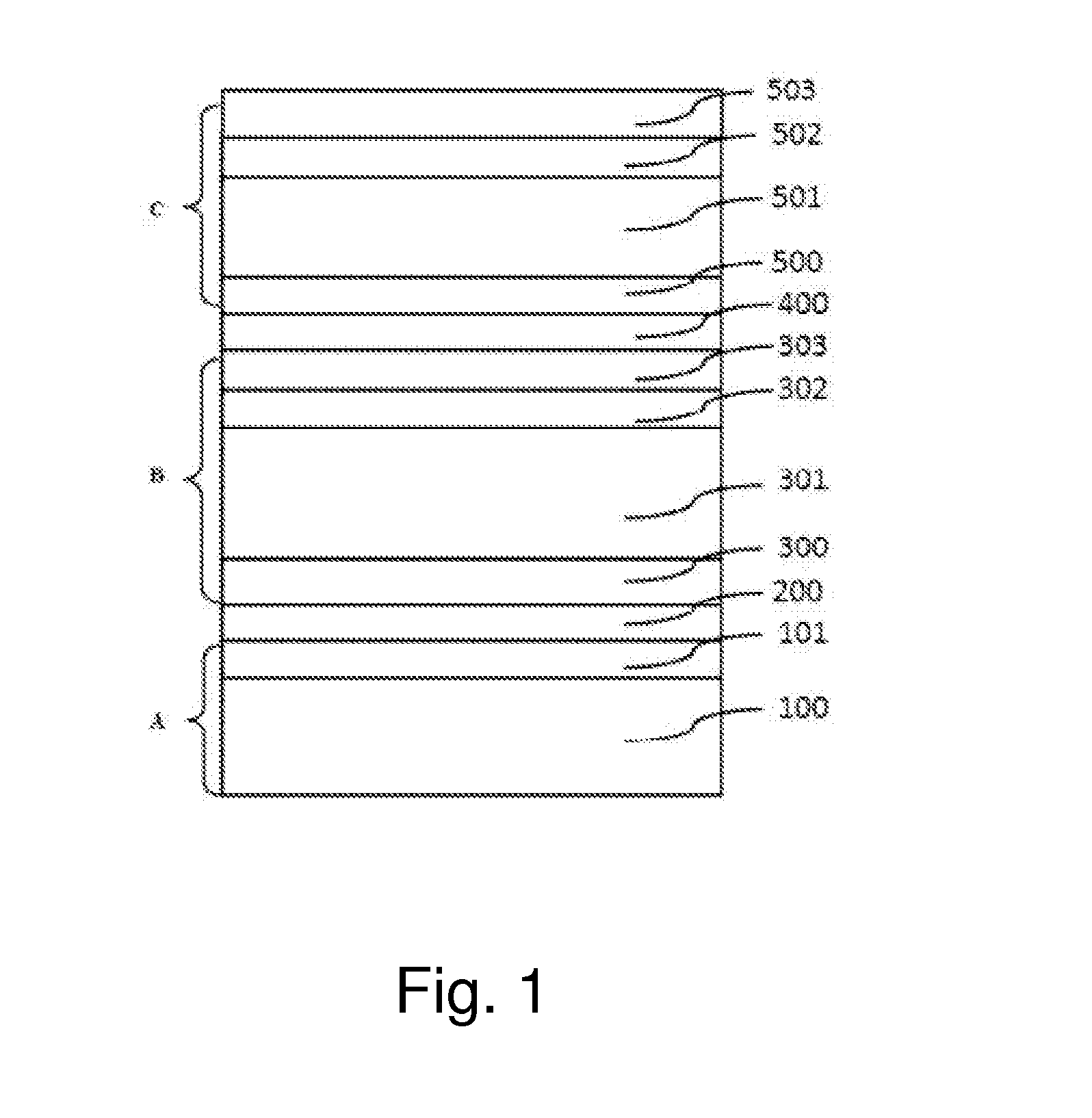
[0038]As illustrated in FIG. 1, a high-concentration multi-junction solar cell comprises a Ge bottom cell A, an intermediate cell B, a top cell C and two tunneling junctions 200 and 400 connecting the cells.

[0039]More specifically, the figure shows: one P-type Ge substrate 100 and one n-type Ga0.5In0.5P window layer 101 deposited on the substrate, which form a Ge bottom cell A.

[0040]A series of highly doped P-type and n-type layers are deposited on the top of the Ge bottom cell A, forming a GaAs tunneling junction 200 and used for connecting the Ge bottom cell A to the intermediate cell B.

[0041]An intermediate cell back surface field layer 300 is deposited on the top of the formed GaAs tunneling junction 200 and used for reducing recombination loss. The layer is preferably formed by P-type AlGaAs.

[0042]An intermediate cell base area 301 and an intermediate cell emitter layer 302 are deposited on an intermediate cell back surface field layer 300. In the preferred embodiment, the inte...

embodiment two

[0046]The embodiment is a fabricating process of the high-concentration multi-junction solar cell in Embodiment One, comprising the process of the sub-cells A, B and C and each layer between the sub-cells. In the course of MOCVD epitaxial growth, by controlling and adjusting the flow ratio of n-type dopant source in the reaction source, the grading of the doping concentration of the emitter layer can be realized.

[0047]The specific fabrication process comprises the following steps:

[0048]The p-type doped Ge substrate 100 has a thickness of 150 micron and functions as the Ge bottom cell base area.

[0049]The P-type Ge substrate 100 is well cleaned and placed in a MOCVD reaction chamber; first the P-type Ge substrate 100 is baked for ten minutes at the temperature of 750° C. and then decreased to a temperature of 600° C. n-type Ga0.5In0.5P window layer 101 grows epitaxially to form the Ge bottom cell A.

[0050]The GaAs tunneling junction 200 connecting the bottom and intermediate cells grow...


PUM


Abstract

A high-concentration multi-junction solar cell and method for fabricating same is provided. The high-concentration multi-junction solar cell comprises a top cell, an intermediate cell, a bottom cell and two tunneling junctions connecting the top cell and intermediate cell and the intermediate cell and bottom cell. The emitter layers of the top and intermediate cells both employ the graded doping concentrations and have high open circuit voltage and short circuit current. The top cell emitter layer is over several hundred nanometers thicker than that of the traditional multi-junction cell so as to decrease the whole series resistance of the multi-junction cell, improve the fill factor, and gain higher photoelectric conversion efficiency.

Description

CROSS-REFERENCE TO RELATED APPLICATIONS[0001]This application claims priority to PCT / CN2012 / 075134 filed on May 7, 2012 and published on Dec. 27, 2012 as publication WO 2012 / 174952, which claims priority to Chinese Patent Application No. 201110168522.9 entitled “High-concentration multi-junction solar cell and method for fabricating same”, filed on Jun. 22, 2011, the contents of which are incorporated herein by reference in its entirety.FIELD OF THE INVENTION[0002]This invention pertains to the field of compound semiconductor solar cell, and specifically relates to a high-concentration multi-junction solar cell and a method for fabricating the same.BACKGROUND OF THE INVENTION[0003]The photovoltaic power generation technology, after the development of the first-generation crystalline silicon cells and the second-generation thin film photovoltaic cells, is now entering upon an age of the second-generation concentrated photovoltaic (CPV) technology. III-V concentrating multi-junction s...

Claims


Application Information

Patent Timeline
Patent Type & Authority Applications(United States)
IPC IPC(8): H01L31/0687H01L31/0725
CPCH01L31/0725H01L31/0687Y02E10/544Y02P70/50
Inventor SONG, MINGHUILIN, GUIJIANGWU, ZHIHAOWANG, LIANGJUNLIU, JIANQINGBI, JINGFENGXIONG, WEIPINGLIN, ZHIDONG
Owner XIAMEN SANAN OPTOELECTRONICS TECH CO LTD
Why Eureka
Try Eureka