Semiconductor alloy fin field effect transistor

a technology of semiconductor alloy and transistor, applied in the direction of semiconductor devices, electrical equipment, basic electric elements, etc., can solve the problems of forming a semiconductor alloy material on a semiconductor substrate, and generating an undesirable

Active Publication Date: 2014-04-10
GLOBALFOUNDRIES US INC
View PDF5 Cites 38 Cited by
  • Summary
  • Abstract
  • Description
  • Claims
  • Application Information

AI Technical Summary

Benefits of technology

[0003]Semiconductor alloy fin structures can be formed by recessing a semiconductor material layer including a first semiconductor material to form a trench, and epitaxially depositing a semiconductor alloy material of the first semiconductor material and a second semiconductor material within the trench. The semiconductor alloy material is epitaxially aligned to the first semiconductor material in the semiconductor material layer. First semiconductor fins including the first ...

Problems solved by technology

However, forming a semiconductor alloy material on a semiconductor substrate is prone to generating an undesirable lateral...

Method used


Image

  • Semiconductor alloy fin field effect transistor
  • Semiconductor alloy fin field effect transistor
  • Semiconductor alloy fin field effect transistor

Examples


first embodiment

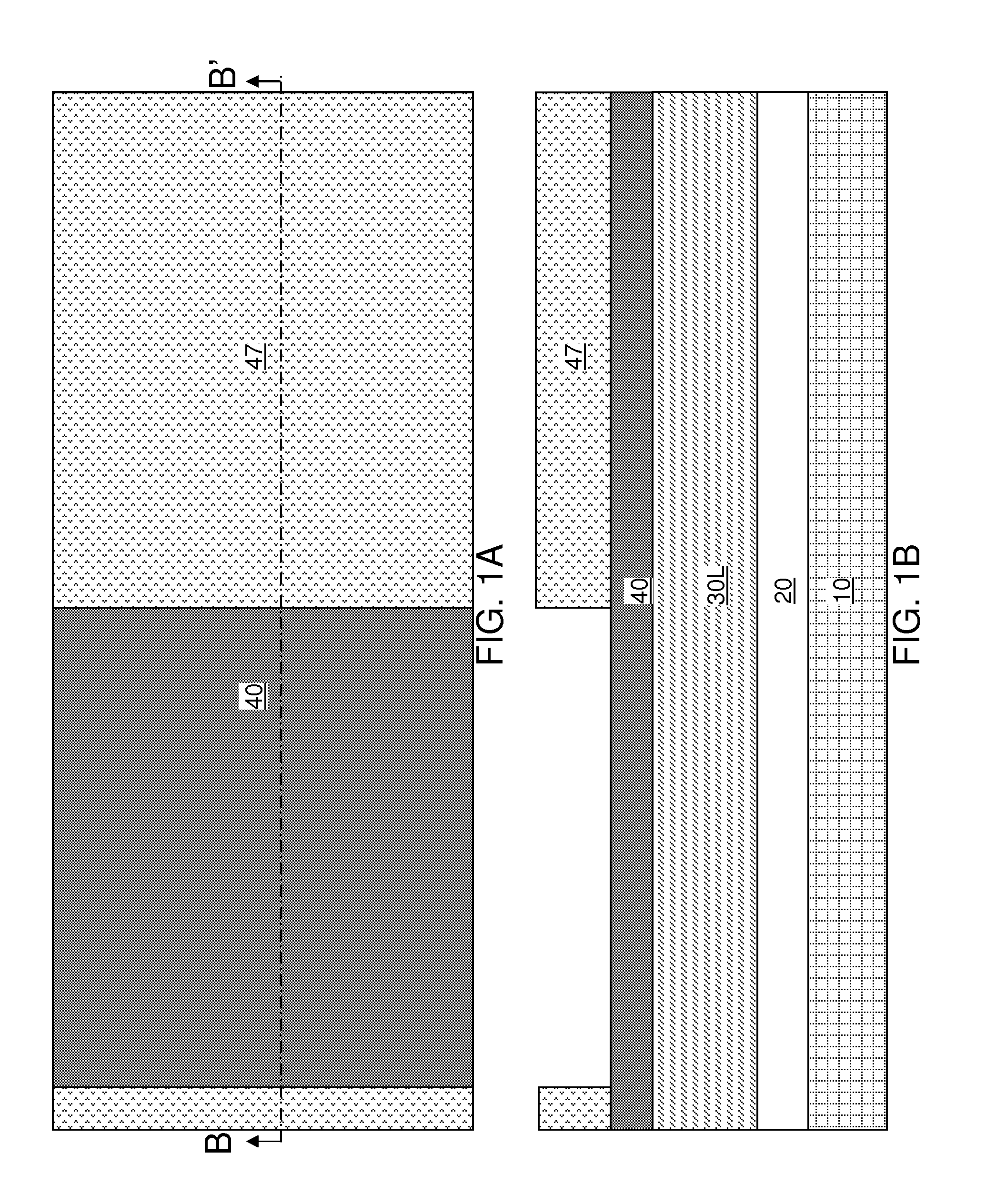
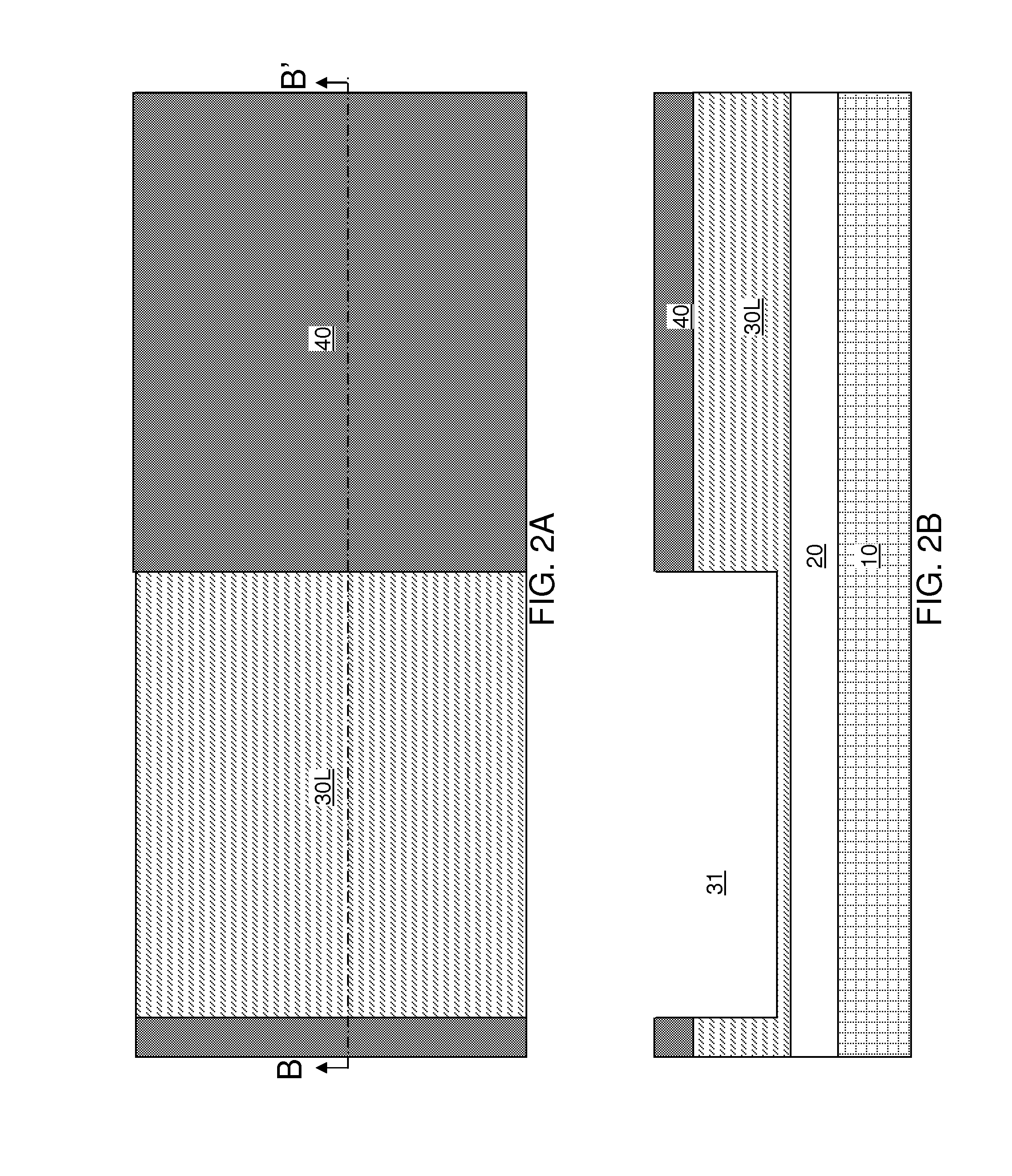
[0038]Referring to FIGS. 1A and 1B, a first exemplary semiconductor structure according to the present disclosure can be formed by providing a semiconductor-on-insulator (SOI) substrate. The SOI substrate can include a vertical stack, from bottom to top, of a handle substrate 10, a buried insulator layer 20, and a top semiconductor layer 30L.

[0039]The handle substrate 10 can include a semiconductor material, a conductive material, and / or a dielectric material. The handle substrate 10 provides mechanical support to the buried insulator layer 20 and the top semiconductor layer 30L. The thickness of the handle substrate 10 can be from 30 microns to 2 mm, although lesser and greater thicknesses can also be employed.

[0040]The buried insulator layer 20 includes a dielectric material such as silicon oxide, silicon nitride, silicon oxynitride, or a combination thereof. The thickness of the buried insulator layer 20 can be from 50 nm to 5 microns, although lesser and greater thicknesses can ...

second embodiment

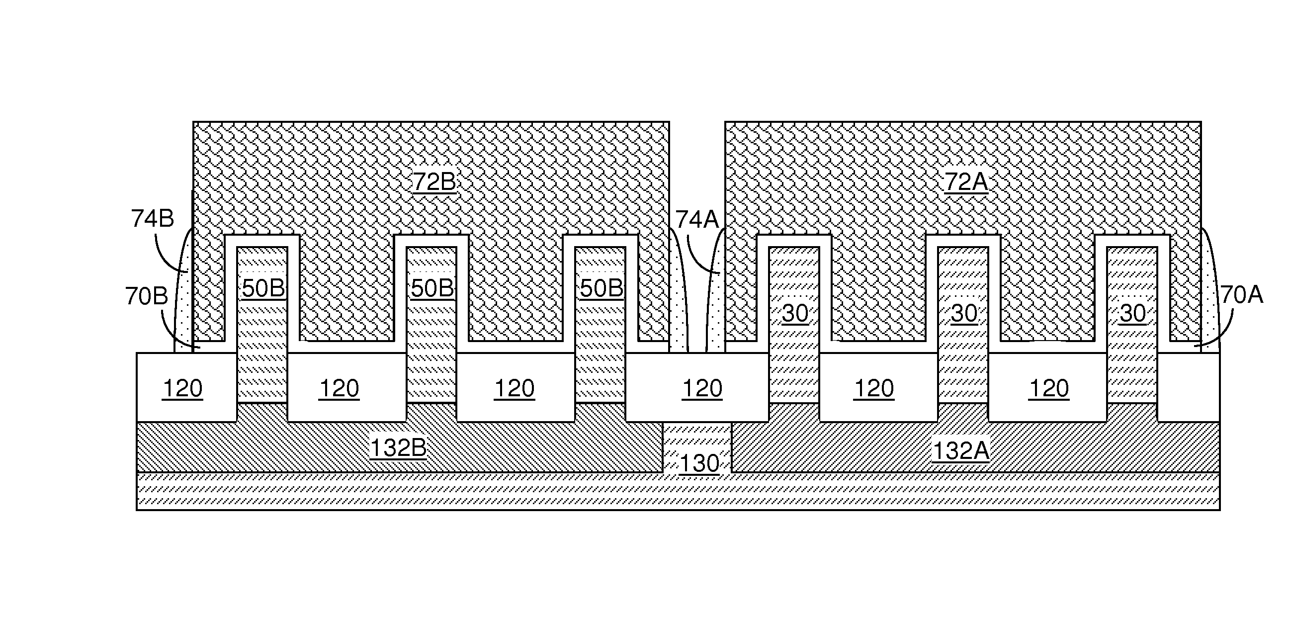
[0064]Referring to FIGS. 9A and 9B, a second exemplary semiconductor structure according to the present disclosure can be formed employing a bulk semiconductor substrate including a single crystalline semiconductor layer 130L. The single crystalline semiconductor layer 130L includes a first semiconductor material throughout an entirety thereof. The entirety of the single crystalline semiconductor layer 130L is single crystalline.

[0065]A first embedded doped well 132A and a second embedded doped well 132B can be formed within the single crystalline semiconductor layer 130L. In one embodiment, the first embedded doped well 132A and the second embedded doped well 132B may have a doping of opposite conductivity types. For example, the first embedded doped well 132A can be a p-doped well and the second embedded doped well 132B can be an n-doped well, or vice versa. The dopant concentration of the first embedded doped well 132A and the second embedded doped well 132B can be in any range k...


PUM


Abstract

Semiconductor alloy fin structures can be formed by recessing a semiconductor material layer including a first semiconductor material to form a trench, and epitaxially depositing a semiconductor alloy material of the first semiconductor material and a second semiconductor material within the trench. The semiconductor alloy material is epitaxially aligned to the first semiconductor material in the semiconductor material layer. First semiconductor fins including the first semiconductor material and second semiconductor fins including the semiconductor alloy material can be simultaneously formed. In one embodiment, the first and second semiconductor fins can be formed on an insulator layer, which prevents diffusion of the second semiconductor material to the first semiconductor fins. In another embodiment, shallow trench isolation structures and reverse biased wells can be employed to provide electrical insulation among neighboring semiconductor fins.

Description

BACKGROUND[0001]The present disclosure relates to a semiconductor structure, and more particularly to a semiconductor structure including semiconductor fins containing an alloy of two semiconductor materials, and a method of manufacturing the same.[0002]A semiconductor alloy material including at least two semiconductor materials can provide a performance advantage for a field effect transistor. For example, a silicon germanium alloy channel can provide enhanced on-current over a silicon channel for p-type field effect transistors. However, forming a semiconductor alloy material on a semiconductor substrate is prone to generating an undesirable lateral diffusion of semiconductor materials into neighboring semiconductor material regions requiring a single semiconductor material.BRIEF SUMMARY[0003]Semiconductor alloy fin structures can be formed by recessing a semiconductor material layer including a first semiconductor material to form a trench, and epitaxially depositing a semicondu...

Claims


Application Information

Patent Timeline
IPC IPC(8): H01L29/06H01L21/20
CPCH01L29/66068H01L29/66795H01L29/785H01L21/0262H01L21/02636H01L21/02529H01L21/02532H01L21/823821H01L21/845H01L27/1211H01L29/16H01L27/0886H01L29/0649H01L29/1608H01L29/161H01L29/165H01L29/7851
Inventor CHENG, KANGGUOADAM, THOMAS N.KHAKIFIROOZ, ALIREZNICEK, ALEXANDER
Owner GLOBALFOUNDRIES US INC
Why Eureka
Try Eureka