Light-emitting device and method for manufacturing the same
a technology of light-emitting devices and manufacturing methods, which is applied in the direction of semiconductor/solid-state device manufacturing, semiconductor devices, electrical equipment, etc., can solve the problems of large current flow, crosstalk phenomenon, deterioration of organic el elements, etc., and achieve suppressing the occurrence of crosstalk phenomena, wide process margins, and suppressing the effect of crosstalk phenomena
- Summary
- Abstract
- Description
- Claims
- Application Information
AI Technical Summary
Benefits of technology
Problems solved by technology
Method used
Image
Examples
embodiment 1
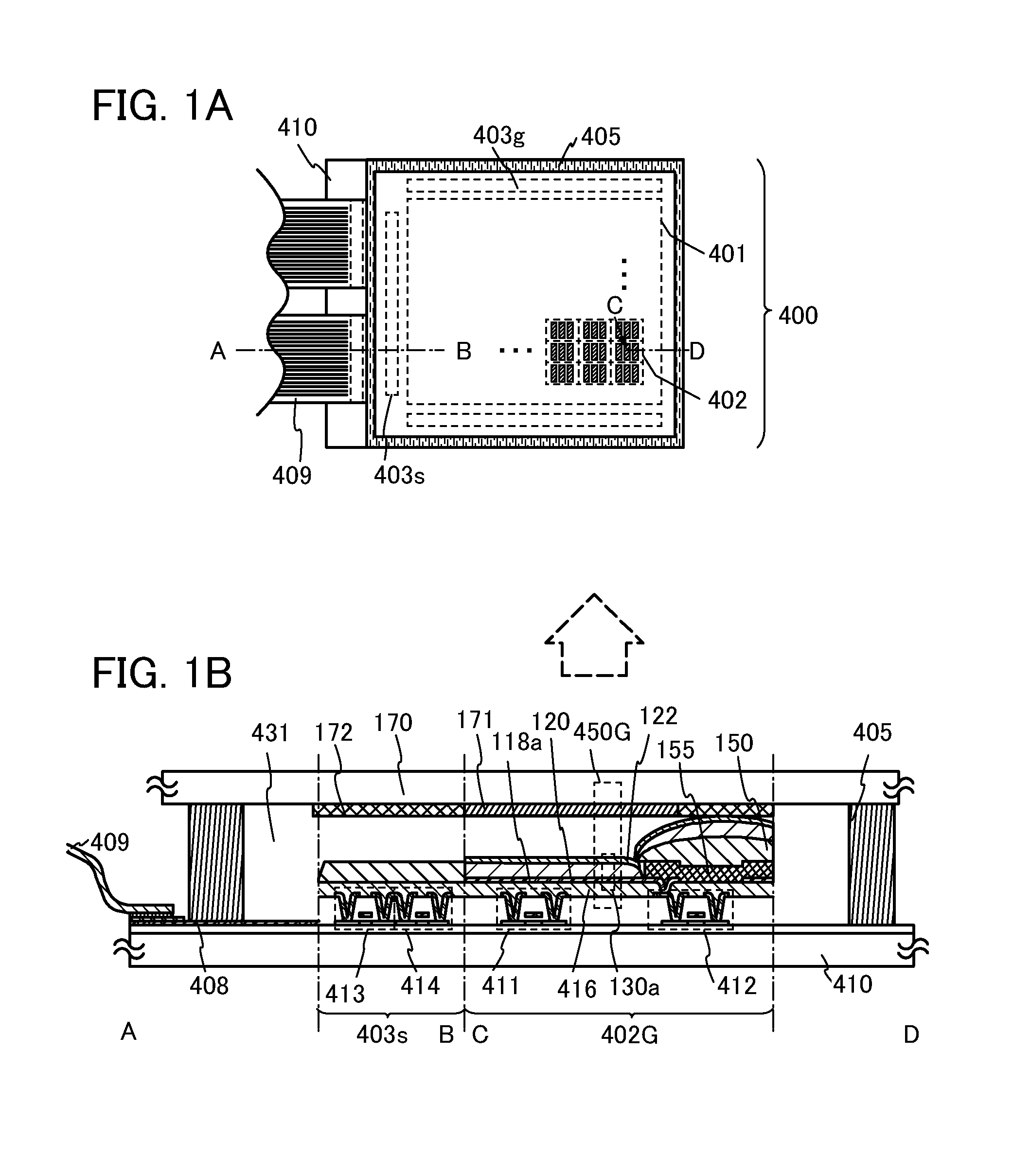
[0052]FIGS. 1A and 1B illustrate a structure of a display panel which can be used for a display device in one embodiment of the present invention. FIG. 1A is a top view of the structure of the display panel which can be used for a display device in one embodiment of the present invention, and FIG. 1B is a side view of the structure including cross sections along section lines A-B and C-D in FIG. 1A.
[0053]A display panel 400 shown as an example in this embodiment includes a display portion 401 over a first substrate 410. The display portion 401 includes a plurality of pixels 402. The pixel 402 includes a plurality of sub-pixels (e.g., three sub-pixels) (see FIG. 1A). Over the first substrate 410, in addition to the display portion 401, a source side driver circuit portion 403s and a gate side driver circuit portion 403g which drive the display portion 401 are provided. Note that the driver circuit portions can be provided not over the first substrate 410 but externally.
[0054]The disp...
example 1
[0123]Lower electrode: silver, silver-magnesium alloy, indium tin oxide (ITO), or metal oxide in which indium is mixed with zinc oxide
[0124]Conductive sacrifice layer: Al or Al alloy
[0125]Etchant: photoresist developer (alkali metal such as tetramethyl ammonium hydroxide (TMAH))
[0126]Partition: acrylic-based resin, polyimide-based resin, siloxane-based resin, phenol-based resin, novolac-based resin, or the like
example 2
[0127]Lower electrode: ITO, Ti oxide, or the like
[0128]Conductive sacrifice layer: indium zinc oxide
[0129]Etchant: oxalic acid etchant
[0130]Partition: acrylic-based resin, polyimide-based resin, siloxane-based resin, phenol-based resin, novolac-based resin, or the like
PUM
| Property | Measurement | Unit |
|---|---|---|
| wavelength | aaaaa | aaaaa |
| wavelength | aaaaa | aaaaa |
| wavelength | aaaaa | aaaaa |
Abstract
Description
Claims
Application Information


