Copper-Titanium Alloy Sputtering Target, Semiconductor Wiring Line Formed Using the Sputtering Target, and Semiconductor Element and Device Each Equipped with the Semiconductor Wiring Line

a technology of sputtering target and copper alloy, which is applied in the direction of electrolysis components, vacuum evaporation coatings, coatings, etc., can solve the problems of unavoidable formation of diffusion barrier layers made of ta or tan, copper contamination of semiconductor si substrate, and unsatisfactory means, so as to improve the em resistance, prevent contamination around the wiring line, and improve the effect of corrosion resistan

Inactive Publication Date: 2014-04-24
JX NIPPON MINING& METALS CORP
View PDF1 Cites 5 Cited by
  • Summary
  • Abstract
  • Description
  • Claims
  • Application Information

AI Technical Summary

Benefits of technology

[0028]The copper alloy wiring line for semiconductors and the sputtering target for forming the foregoing wiring line according to the present invention yield superior effects of being able to cause the copper alloy wiring line for semiconductors to be equipped with a self-diffusion suppressive

Problems solved by technology

While copper or copper alloy is extremely useful as a wiring line material for semiconductors, since copper itself is an extremely active metal that diffuses easily, there is a problem in that copper contaminates the semiconductor Si substrate, or contaminates the Si substrate or the periphery thereof through the insulating film formed on the Si substrate.
Thus, with conventional technologies, the formation of a diffusion barrier layer made of Ta or TaN is an unavoidable process.
Nevertheless, this is not necessarily the ideal means since there is the problem of the number of processes increasing by that much.
Thus, in substitute for this diffusion barrier layer, proposed is depositing a co

Method used


Image

  • Copper-Titanium Alloy Sputtering Target, Semiconductor Wiring Line Formed Using the Sputtering Target, and Semiconductor Element and Device Each Equipped with the Semiconductor Wiring Line
  • Copper-Titanium Alloy Sputtering Target, Semiconductor Wiring Line Formed Using the Sputtering Target, and Semiconductor Element and Device Each Equipped with the Semiconductor Wiring Line
  • Copper-Titanium Alloy Sputtering Target, Semiconductor Wiring Line Formed Using the Sputtering Target, and Semiconductor Element and Device Each Equipped with the Semiconductor Wiring Line

Examples


example 1

[0061]In order to produce a sputtering target comprising 3.0 at % of Ti and a remainder made up of Cu, used as the raw materials were Cu having a purity of 6N and Ti having a purity of 5N.

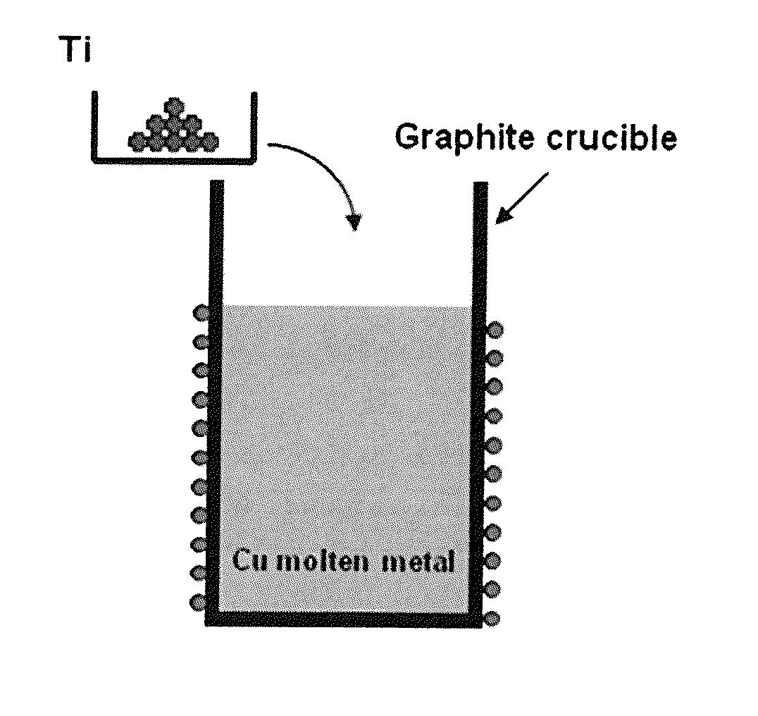
[0062]Copper was melted via vacuum induction melting. 32187 g of copper was used, and the vacuum degree was set to 0.05 Pa. After melting Cu, the molten metal was retained at 1100 to 1250° C., Ar gas was introduced, and Ti was added. Agitation was performed via natural convection. Time from the addition of Ti to metal tapping was 12 minutes. A copper mold was used, the tapping temperature was set to 1100 to 1250° C., and the molten metal was solidified therein.

[0063]The solidified ingot was subject to forging at 700 to 950° C., and the thickness was thereby reduced from 100 mmt to 70 mmt. This was further subject to hot rolling at 700 to 950° C., and the thickness was further reduced from 70 mmt to 12 mmt. Subsequently, this was subject to heat treatment at 700 to 950° C.×1 hr.

[0064]In addition, th...

example 2

[0070]In order to produce a sputtering target comprising 5.0 at % of Ti and a remainder made up of Cu, used as the raw materials were Cu having a purity of 6N and Ti having a purity of 5N.

[0071]Copper was melted via vacuum induction melting. 32187 g of copper was used, and the vacuum degree was set to 0.05 Pa. After melting Cu, the molten metal was retained at 1100 to 1250° C., Ar gas was introduced, and Ti was added. Agitation was performed via natural convection. Time from the addition of Ti to metal tapping was 12 minutes. A copper mold was used, the tapping temperature was set to 1100 to 1250° C., and the molten metal was solidified therein.

[0072]The solidified ingot was subject to forging at 700 to 950° C., and the thickness was thereby reduced from 100 mmt to 70 mmt. This was further subject to hot rolling at 700 to 950° C., and the thickness was further reduced from 70 mmt to 12 mmt. Subsequently, this was subject to heat treatment at 700 to 950° C.×1 hr.

[0073]In addition, th...

example 3

[0080]In order to produce a sputtering target comprising 7.0 at % of Ti and a remainder made up of Cu, used as the raw materials were Cu having a purity of 6N and Ti having a purity of 5N.

[0081]Copper was melted via vacuum induction melting. 32187 g of copper was used, and the vacuum degree was set to 0.05 Pa. After melting Cu, the molten metal was retained at 1100 to 1250° C., Ar gas was introduced, and Ti was added. Agitation was performed via natural convection. Time from the addition of Ti to metal tapping was 12 minutes. A copper mold was used, the tapping temperature was set to 1100 to 1250° C., and the molten metal was solidified therein.

[0082]The solidified ingot was subject to forging at 700 to 950° C., and the thickness was thereby reduced from 100 mmt to 70 mmt. This was further subject to hot rolling at 700 to 950° C., and the thickness was further reduced from 70 mmt to 12 mmt. Subsequently, this was subject to heat treatment at 700 to 950° C.×1 hr. In addition, this wa...


PUM

PropertyMeasurementUnit
Grain sizeaaaaaaaaaa

Abstract

A copper-titanium alloy sputtering target comprising 3 at % or more and less than 15 at % of Ti and a remainder made up of Cu and unavoidable impurities, wherein a variation (standard deviation) in hardness is within 5.0 and a variation (standard deviation) in electric resistance is within 1.0 in an in-plane direction of the target. Provided are: a sputtering target for forming a copper-titanium alloy wiring line for semiconductors capable of causing the copper alloy wiring line for semiconductors to be equipped with a self-diffusion suppressive function, effectively preventing contamination around the wiring line caused by diffusion of active Cu, improving electromigration (EM) resistance, corrosion resistance and the like, enabling the arbitrary formation of a barrier layer in a simple manner, and uniformizing film properties; a copper-titanium alloy wiring line for semiconductors; and a semiconductor element and a device each equipped with the semiconductor wiring line.

Description

TECHNICAL FIELD[0001]The present invention relates to a sputtering target for forming a copper alloy wiring line for semiconductors capable of effectively preventing contamination around the wiring line caused by diffusion of active Cu, and particularly relates to a copper-titanium (Cu—Ti) alloy sputtering target suitable for forming a semiconductor wiring line equipped with a self-diffusion suppressive function, a copper-titanium alloy sputtering target capable of uniform sputter deposition and thereby obtaining uniform film properties, a semiconductor wiring line formed using the foregoing sputtering target, and a semiconductor element and a device each equipped with the foregoing semiconductor wiring line.BACKGROUND ART[0002]Conventionally, Al alloy (specific resistance of roughly 3.0 μΩ·cm) had been used as the wiring line material of a semiconductor element, but pursuant to finer wiring lines, a copper wiring line with lower resistance (specific resistance of roughly 1.7 μΩ·cm)...

Claims


Application Information

Patent Timeline
IPC IPC(8): H01L23/532C23C14/34
CPCH01L23/53233H01L23/53261C23C14/3407C23C14/165C23C14/3414H01L23/53238C22C9/00C22F1/08H01L2924/0002C22C1/02H01L2924/00C23C14/34H01L21/28H01L21/285H01L21/3105H01L23/52
Inventor OTSUKI, TOMIOFUKUSHIMA, ATSUSHI
Owner JX NIPPON MINING& METALS CORP
Why Eureka
Try Eureka