Methods for Selective and Conformal Epitaxy of Highly Doped Si-containing Materials for Three Dimensional Structures

a highly doped, conformal technology, applied in the direction of basic electric elements, electrical apparatus, semiconductor devices, etc., can solve the problems of increasing the subthreshold leakage at the corners, no viable option of continuing, and deposition of epitaxy materials, and achieve excellent crystal quality

Inactive Publication Date: 2014-05-01
MATHESON TRI GAS INC
View PDF0 Cites 326 Cited by
  • Summary
  • Abstract
  • Description
  • Claims
  • Application Information

AI Technical Summary

Benefits of technology

[0017]Deposition and / or growth methods have now been developed for the fabrication of FinFET devices that utilize a silicon source, such as, higher order silanes including straight and isomeric forms, such as, but not limited to tetrasilane (n-tetrasilane, iso-tetrasilane and cyclo-tetrasilane). The Si epitaxial layer is required to provide conformal deposition thickness and conformal doping profile with excellent crystal quality on different surface orientations (i.e., Si (100) vs Si (110) due to device performance design. To enhance the junction between the channel and source drain and / or between the source drain and contact (silicide formation), Fin structure to be thick by doped Si epitaxial process.
[0018]Another fabrication technique provides a method for minimizing the defect levels on all exposed Si crystallographic planes and thereby obtaining equivalent growth on all exposed planes. This is accomplished be by tailoring the cyclical deposition / etching (CDE) net growth rate.

Problems solved by technology

As scaling continued down to the 65 nm, 45 nm, etc. nodes, it became apparent that there was no viable options of continuing forth with the conventional (planar) MOSFET, resulting in the development of the double gate MOSFET (DG-FET) and triple gate MOSFET.
As a result, there is increased subthreshold leakage at the corners.
Amongst the DG-FET types, the FinFET is the easiest one to fabricate; however, the fabrication of the uniform, ultra thin fins is one of the key challenges in FinFET fabrication.
Therefore, by changing the concentration of an etchant gas, the net selective process results in deposition of epitaxy material and limited, or no, deposition of polycrystalline material.
On the other hand, the ultra shallow source / drain junction inevitably results in increased series resistance.
Also, junction consumption during silicide formation increases the series resistance even further.
However, current selective epitaxy processes have some drawbacks.
Such high temperatures are not desirable during a fabrication process due to thermal budget considerations and possible uncontrolled nitridation reactions to the substrate surface.
In situ doping is often preferred over ex situ doping followed by annealing to incorporate the dopant into the lattice structure because the annealing may undesirably consume thermal budget.
However, in practice in situ substitutional carbon doping is complicated by the tendency for the dopant to incorporate non-substitutionally during deposition, e.g., interstitially in domains or clusters within the silicon, rather than by substituting for silicon atoms in the lattice structure.
Non-substitutional doping also complicates substitutional doping using other material systems, e.g., carbon doping of SiGe, doping of Si and SiGe with electrically active dopants, etc.
However, prior deposition methods are not known to have been successful for depositing single crystal silicon having an in situ doped substitutional carbon content of greater than 2.3 atomic %.

Method used


Image

  • Methods for Selective and Conformal Epitaxy of Highly Doped Si-containing Materials for Three Dimensional Structures
  • Methods for Selective and Conformal Epitaxy of Highly Doped Si-containing Materials for Three Dimensional Structures
  • Methods for Selective and Conformal Epitaxy of Highly Doped Si-containing Materials for Three Dimensional Structures

Examples


example 1

Tetrasilane CDE Net Growth Per Cycle Impact on FinFET Crystallographic Planes

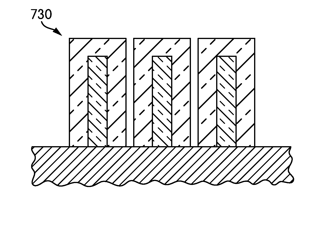
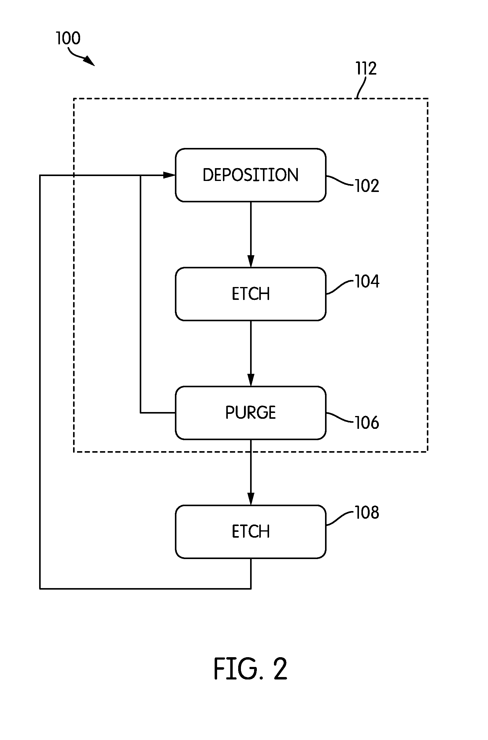
[0088]As discussed previously, normal selective epitaxial growth (SEG) utilizing dichlorosilane chemistry (DSC) typically results in a saw-tooth morphology 300, as seen in FIG. 3A. It has been discovered that by controlling tetrasilane cycle deposition etch (CDE) net growth per cycle no defective layers is obtained for FinFET source / drain region and epitaxial doped-silicon growth on in. By using tetrasilane CDE, as disclosed herein, good morphology doped-silicon growth is achieved on the FIN and no facet formation under silicide layer is apparent. This ultimately has a benefit of reducing contact resistivity.

[0089]In order to reduce the net growth per cycle. (5-25 Å / cycle) there are two methods. First growth thickness may be reduced by deposition time or growth rate and second, increase etched thickness by etching time or etch rate. Both methods or a combination of the two are effective at reducing the net ...

example 2

Process for the Production of Highly Doped SiAs Epitaxy Layer

[0096]The present invention describes N-type doping with tetrasilane as Si precursor, eliminates the N type doping surface segregation, growth rate poisoning effect. Reducing these effects thus leads to same growth rates and doping concentrations on both 100 and 110 crystallographic planes. Cyclical deposition and etch (CDE) reduces defect level.

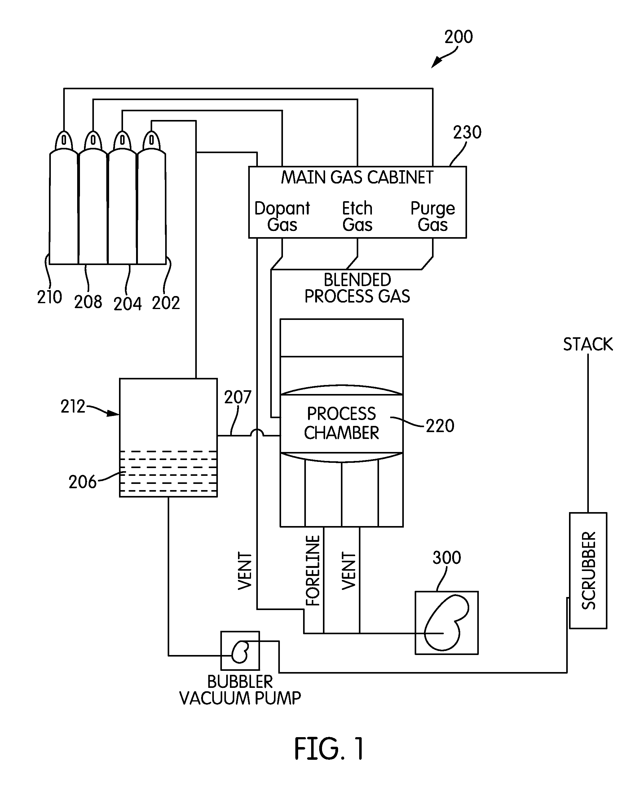
[0097]After loading a substrate into the process chamber, the conditions in the process chamber are adjusted to a predetermined temperature and pressure. In this particular example the process chamber is maintained at a temperature below about 550° C. during deposition and etching. The process chamber was maintained at a pressure of about 10 Torr. The pressure may fluctuate during and between process steps, but is generally maintained constant.

[0098]During the deposition process the substrate is exposed to a tetrasilane to form an epitaxial layer at a rate of about 20 sccm (0.11 g / ...

example 3

Obtaining Selectivity and Uniform Fin Merge with CDE

[0104]As discussed previously, the fabrication of uniform, ultra thin fins is one of the key challenges in FinFET fabrication. Due to non-ideal anisotropic over etch, the epitaxial layer 601 deposited on the fins 604, 604′ and 604″ can end up having a slightly triangular shape whereby voids 607 are created especially at the bottom of the Fins. Once the facets merge at the top 606, the reactant gases cannot reach the bottom of the Fin resulting in voids 607, see FIG. 6A. Concave and convex surfaces can also end up during typical fabrication processes.

[0105]In an embodiment, according to the present invention a uniform Fin merge 610 is achieved during the higher silane CDE process by etching back the Fins 602 at certain intervals during the CDE process thereby selectively targeting the top of the epi growth 602′ thus keeping a space 605 between the fins 604, 604′ and 604″ open so a bottom up fill can occur, see FIG. 6B. This etch bac...


PUM

PropertyMeasurementUnit
temperatureaaaaaaaaaa
pressureaaaaaaaaaa

Abstract

The present invention addresses the key challenges in FinFET fabrication, that is, the fabrications of thin, uniform fins and also reducing the source / drain series resistance. More particularly, this application relates to FinFET fabrication techniques utilizing tetrasilane to enable conformal deposition with high doping using phosphate, arsenic and boron as dopants thereby creating thin fins having uniform thickness (uniformity across devices) as well as smooth, vertical sidewalls, while simultaneously reducing the parasitic series resistance.

Description

CROSS REFERENCE TO OTHER APPLICATIONS[0001]This application claims benefit of priority to U.S. Provisional Application Nos. 61 / 795,992, 61 / 795,993, 61 / 795,994 and 61 / 795,995 all of which were filed on Oct. 29, 2012, the disclosures of which are fully incorporated herein by reference.BACKGROUND OF THE INVENTION[0002]1. Field of the Invention[0003]The present invention addresses the key challenges in the fabrication of three-dimensional structures, that is, the fabrications of thin, uniform fins and also reducing the source / drain series resistance. More particularly, this application relates to FinFET fabrication techniques utilizing tetrasilane to enable conformal deposition with high doping using phosphate, arsenic and boron as dopants thereby creating fins having uniform thickness (uniformity across devices) as well as smooth, vertical sidewalls, while simultaneously reducing the parasitic series resistance.[0004]2. Description of the State of the Art[0005]The relentless pursuit of...

Claims


Application Information

Patent Timeline
Patent Type & Authority Applications(United States)
IPC IPC(8): H01L29/66
CPCH01L29/66795H01L21/02529H01L21/02532H01L21/02576H01L21/02579H01L21/0262H01L21/02639
Inventor SHINRIKI, MANABUBRABANT, PAULCHUNG, JR., KEITH
Owner MATHESON TRI GAS INC
Why Eureka
Try Eureka