
Cvd-free, scalable processes for the production of silicon micro- and nanostructures

a technology of micro- and nanostructures, which is applied in the direction of photomechanical treatment originals, instruments, photomechanical equipment, etc., can solve the problems of inability to scale up production, less desirable for large-scale manufacturing, and high cost of tooling for deep reactive ion etching (drie) methods, and the need for a long process time to complete the manufacturing cycl

Active Publication Date: 2014-05-08
BREWER SCI
View PDF1 Cites 6 Cited by
  • Summary
  • Abstract
  • Description
  • Claims
  • Application Information

AI Technical Summary

Benefits of technology

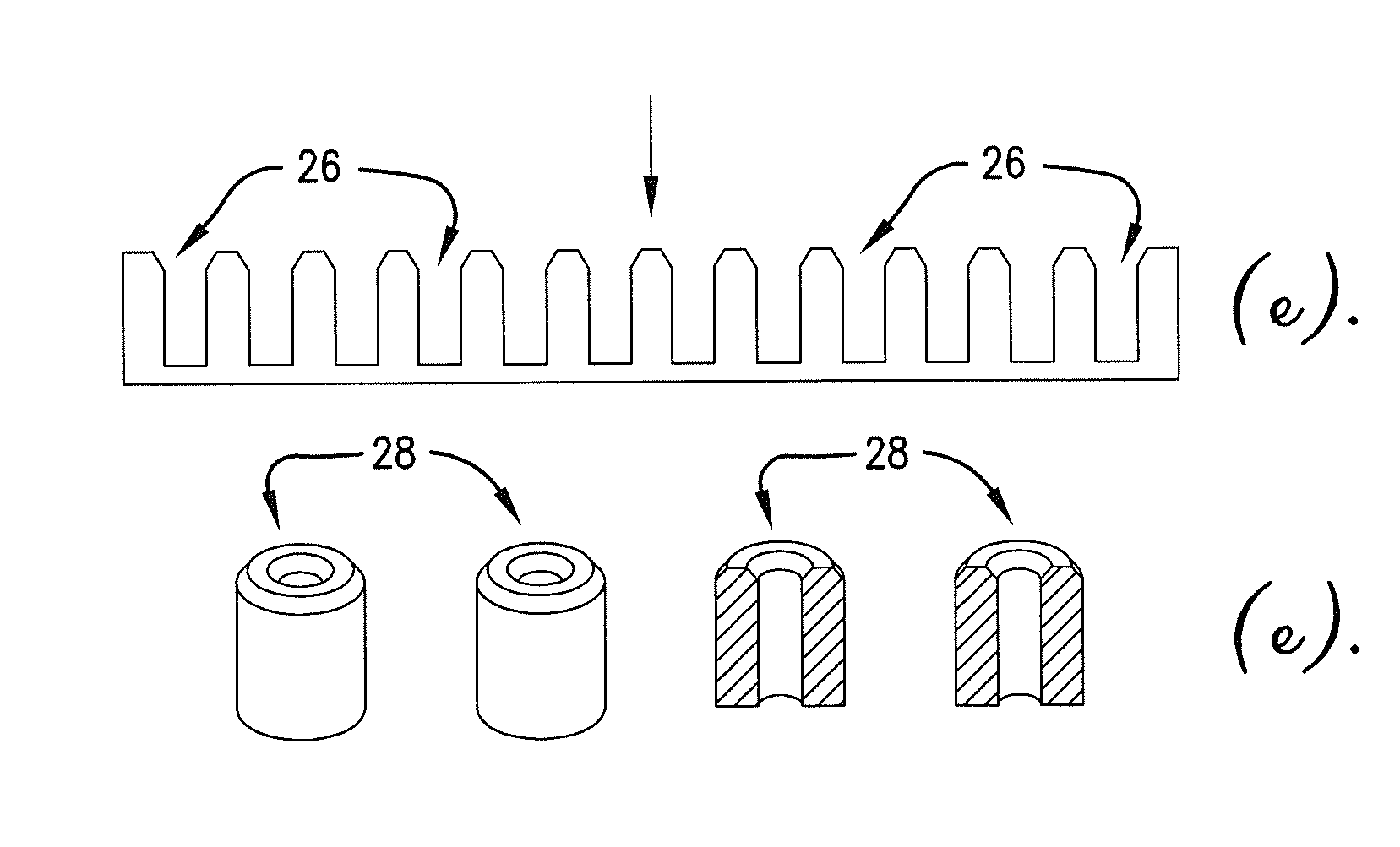
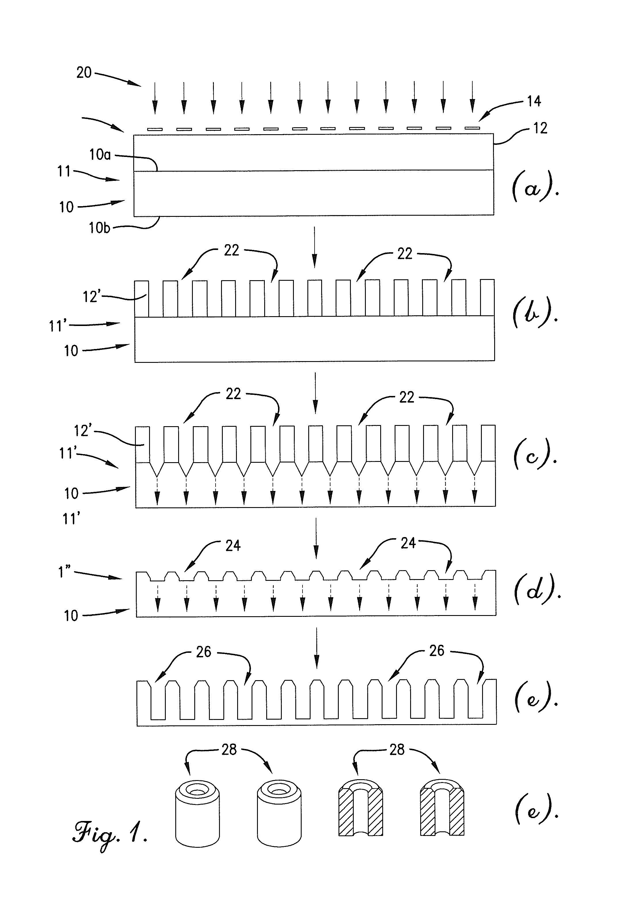
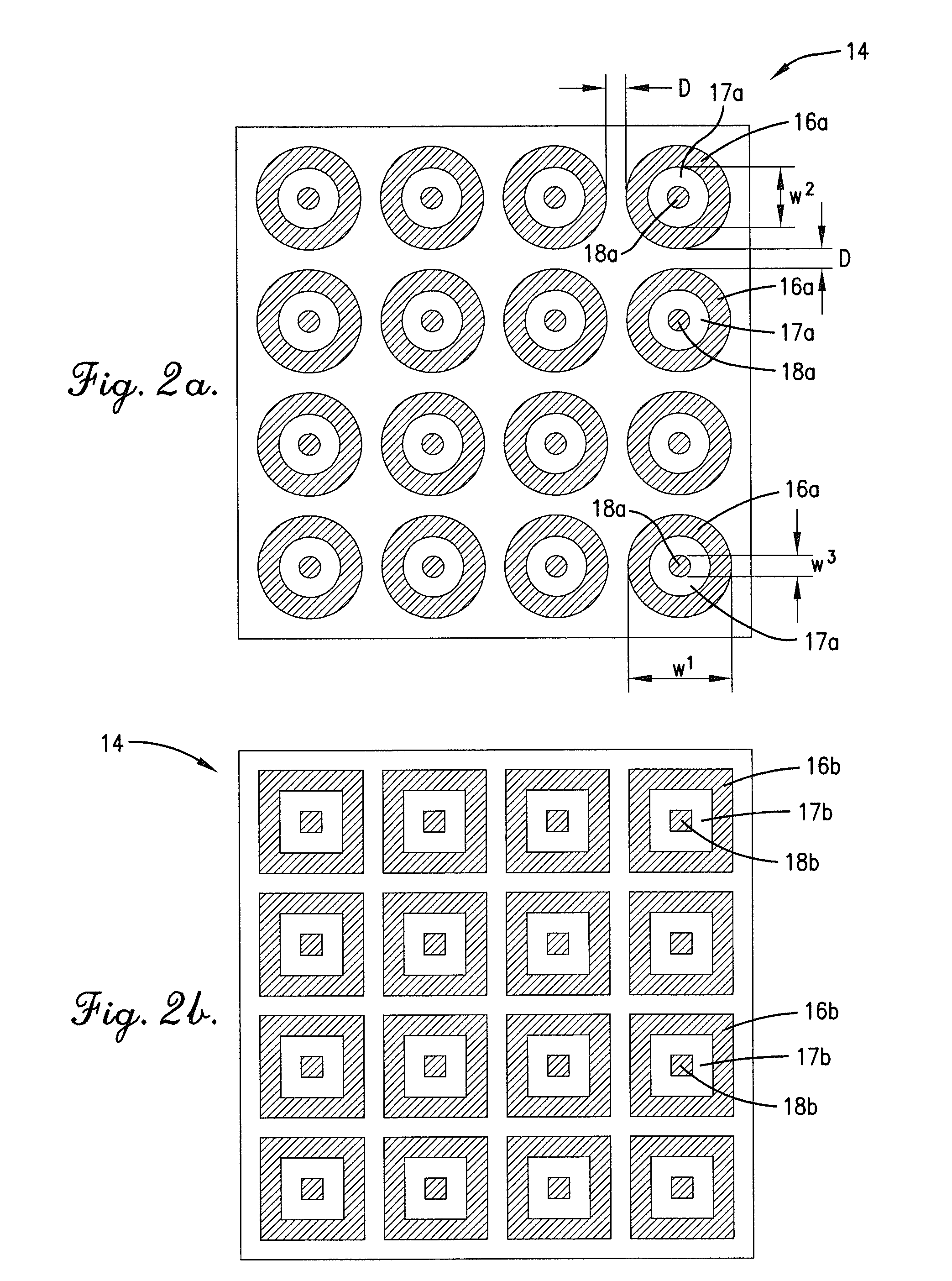
The present invention provides a method for making silicon tubes by forming a pattern in a layer on a silicon substrate and then selectively etching the patterned layer. The result is a patterned surface with silicon tubes. The invention also includes a new mask for use in photolithographic processes. The mask has two different areas of light transmission, which can be used to create the patterned surface with silicon tubes.

Problems solved by technology

Silicon nanostructures are being reported in the literature in laboratory-scale demonstration, but methods to fabricate them incorporate high-temperature (≧320° C.) chemical vapor deposition (CVD) or pyrolysis techniques, which are non-scalable in production.
Other methods, such as metal-assisted etching and electrodeposition, require the use of block copolymers, which involve complex synthesis, making them less desirable for large scale manufacturing.
Deep reactive ion etching (DRIE) methods require expensive tooling and relatively long process times to complete the manufacturing cycle and are, therefore, difficult to scale.
Scanning probe lithography and focused high energy proton beam irradiation are not practical for mass production because patterning speed is slow.

Method used


Image

  • Cvd-free, scalable processes for the production of silicon micro- and nanostructures
  • Cvd-free, scalable processes for the production of silicon micro- and nanostructures
  • Cvd-free, scalable processes for the production of silicon micro- and nanostructures

Examples


example 1

Production of Orderly Array of Microscale Silicon Pores

[0087]A special mask with 4-μm circles was designed. Silicon substrates with low resistivity (1-2 Ω·cm) were used. The silicon substrate was first coated with ProTEK® PSB primer material (Brewer Science, Inc., Rolla, Mo.) at 1,000 rpm and 1,000 rpm / sec for 60 seconds. The primer underlayer was subjected to a two-stage bake, first at 110° C. for 60 seconds and then at 220° C. for 5 minutes. The primer layer was then solvent-stripped by use of a 20-second puddle of PGME (Sigma-Aldrich, St. Louis, Mo.). The silicon wafer with primer layer was then spin dried at 2,000 rpm and 10,000 rpm / sec for 20 seconds. This wafer was then spin-coated with diluted ProTEK® PSB material (11.5% solids, Brewer Science, Inc., Rolla, Mo.) at 1,500 rpm and 1,000 rpm / sec for 60 seconds. The coated wafer was then baked at 110° C. for 120 seconds. The substrate was then exposed on a SUSS mask aligner (broadband exposure at 250 mJ / cm2 measured at 365 nm), f...

example 2

Production of Orderly Array of Microscale Silicon Tubes

[0092]A special mask with 20-μm rings and 5 micron dots was designed to create the outer and inner walls of the tubes, respectively. Silicon substrates with low resistivity (1-2 Ω·cm) were used. Without the use of ProTEK® PSB primer, the silicon wafer was then spin-coated with diluted ProTEK® PSB material (5.75% solids, Brewer Science, Rolla, Mo.) at 1,500 rpm and 1,000 rpm / s for 60 seconds. The coated wafer was then baked at 110° C. for 120 seconds. The substrate was exposed to the outer wall pattern on a SUSS mask aligner (broadband exposure at 250 mJ / cm2, measured at 365 nm), followed by post-exposure bake (PEB) at 110° C. for 2 minutes. Following the PEB, the substrate was developed using ethyl lactate (Sigma-Aldrich, St. Louis, Mo.) for a total of 90 seconds (dynamic dispense, with 5-second on / off dispense). The developed wafer was rinsed with isopropyl alcohol (Sigma-Aldrich, St. Louis, Mo.) for 30 seconds, and a final bak...

example 3

Production of Orderly Array of Microscale Silicon Tubes

[0098]A special mask with 25-μm rings and 5 micron dots was designed to simultaneously create the outer and inner walls of the tubes, respectively. Silicon substrates with low resistivity (1-2 Ω·cm) were used. ProTEK® PSB primer was used as an underlayer. The silicon wafer was spin-coated with diluted ProTEK® PSB primer (Brewer Science, Inc., Rolla, Mo.) at 2,500 rpm and 10,000 rpm / sec for 60 seconds. The coated wafer was then baked at 110° C. for 60 seconds, followed by 220° C. for 5 minutes. The primed wafer was solvent stripped using PGMEA for 52 seconds. The silicon wafer was spin-coated with diluted ProTEK® PSB material (5.75% solids, Brewer Science, Inc., Rolla, Mo.) at 2,500 rpm and 10,000 rpm / sec for 60 seconds. The coated wafer was baked at 110° C. for 120 seconds. The substrate was then exposed to create both outer and inner wall patterns on a SUSS mask aligner (broadband exposure at 250 mJ / cm2 measured at 365 nm), fol...


PUM


Abstract

Manufacturing-friendly and scalable methods for the production of silicon micro- and nanostructures, including silicon nanotubes, are described. The inventive methods utilize conventional integrated circuit and MEMS manufacturing processes, including spin-coating, photolithography, wet and dry silicon etching, and photoassisted electrochemical etch processes. The invention also provides a novel mask, for maximizing the number of tubes obtained per surface area unit of the silicon substrate on which the tubes are built. The resulting tubes have thick and straight outer walls, as well as high aspect ratios.

Description

RELATED APPLICATIONS[0001]This applications claims the priority benefit of U.S. Patent Application No. 61 / 724,116, filed Nov. 8, 2012, entitled CVD-FREE, SCALABLE PROCESSES FOR THE PRODUCTION OF SILICON NANOSTRUCTURES, incorporated by reference herein.BACKGROUND OF THE INVENTION[0002]1. Field of the Invention[0003]The present invention is broadly concerned with the production of silicon micro- and nanostructures, specifically silicon micro- and nanotubes, using standard silicon processing techniques such as lithography and etching.[0004]2. Description of the Prior Art[0005]Silicon micro- and nanostructures (e.g., silicon nanotubes) are of interest for a number of applications, such as for use in high-tech batteries. Silicon nanostructures are being reported in the literature in laboratory-scale demonstration, but methods to fabricate them incorporate high-temperature (≧320° C.) chemical vapor deposition (CVD) or pyrolysis techniques, which are non-scalable in production. Other metho...

Claims


Application Information

Patent Timeline
IPC IPC(8): H01L21/308G03F1/22H01L29/06
CPCH01L21/308G03F1/22H01L29/0676H01L29/0657H01L21/3081B82Y10/00B82Y40/00B81C1/00111B81C99/008G03F1/50G03F7/0035H01L21/0259H01L29/0665H01L29/0669H01L21/02606H10K85/221
Inventor MALHOTRA, JYOTI K.LEITH, JEFFPLANJE, CURTIS
Owner BREWER SCI
Learn More