Fiber-containing resin substrate, device-mounting substrate and device-forming wafer, semiconductor apparatus, and method for producing semiconductor apparatus

Active Publication Date: 2014-05-22
SHIN ETSU CHEM IND CO LTD
View PDF7 Cites 5 Cited by
  • Summary
  • Abstract
  • Description
  • Claims
  • Application Information

AI Technical Summary

Benefits of technology

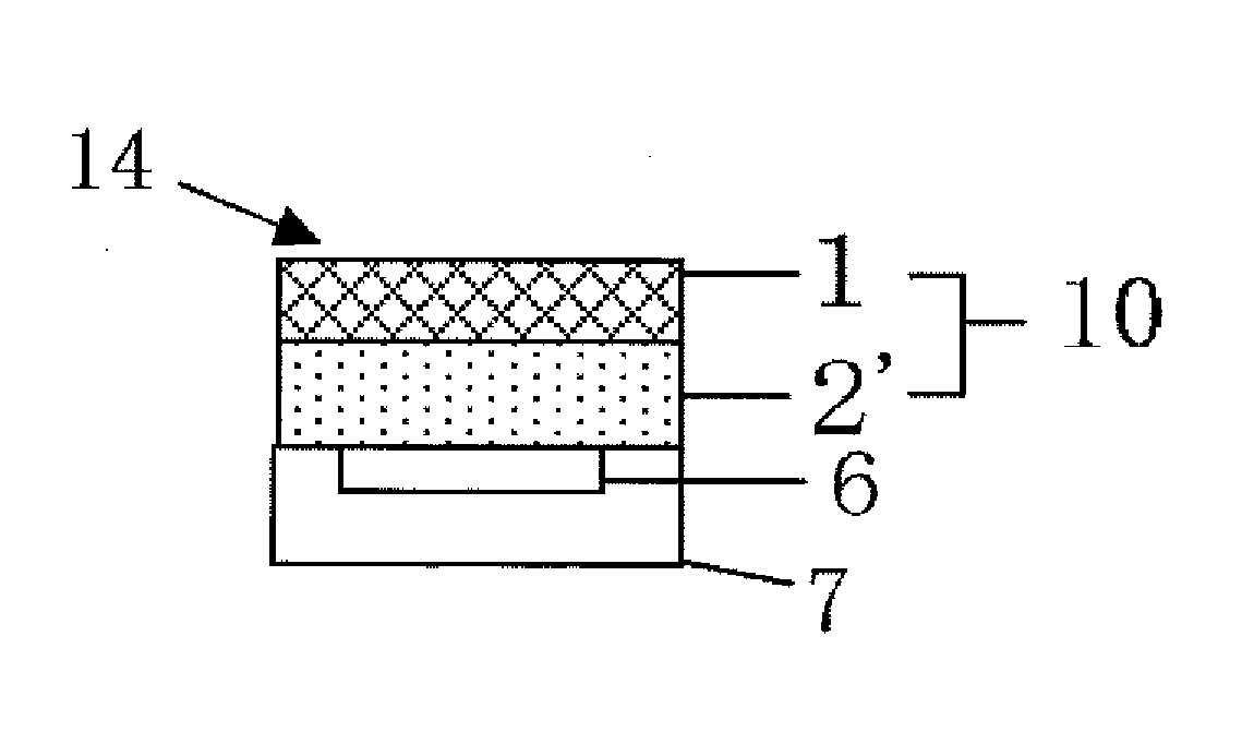
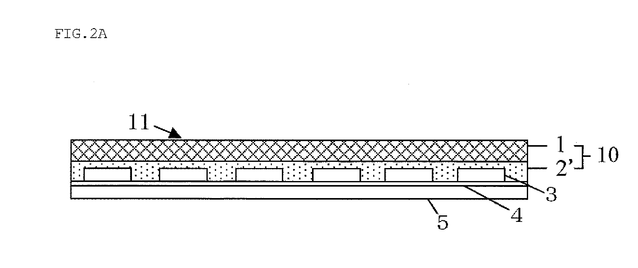
[0029]According to such a method for producing a semiconductor apparatus, the device-mounting surface or the device-forming surface can be readily covered with the uncured resin layer of the fiber-containing resin substrate of the present invention without a failure in filling in the covering step. The method enables the contraction stress of the uncured resin layer to be suppressed during curing by using the resin-impregnated fibrous base material of the of fiber-containing resin substrate, thereby suppressing the warping of the encapsulated substrate or wafer, peeling of the semiconductor devices from the substrate, and the damage of the wafer, and enabling collective encapsulation of the device-mounting surface or the device-forming surface in the encapsulating step. The method can produce a high-quality semiconductor apparatus, because the semiconductor apparatus is cut by dicing into individual pieces from the encapsulated substrate or wafer, which is prevented from warping and encapsulated with the fiber-containing resin substrate exhibiting excellent encapsulation performance, such as heat resistance and humidity resistance after encapsulation, in the cutting step.
[0030]As described above, the fiber-containing resin substrate of the invention can suppress the contraction stress of the uncured resin layer during cu

Problems solved by technology

Such methods enable encapsulation of a wafer or a substrate, such as a metal substrate, having a small diameter, e.g., about 200 mm (8 inches) without a serious problem, whereas encapsulation of the device-mounting surface or device-forming surface of a wafer or a substrate having a large diameter, e.g., 300 mm (12 inches) or more according to these methods brings a serious problem in that the substrate or the wafer is warped, or the wafer is damaged, owing to contraction stress of a resin, such as an epoxy resin, during curing for the encapsulation.
Such contraction stress may disadvantageously cause some of the devices to peel away from the substrate during encapsulating the device-mounting surface of a large-diameter substrate on a wafer level, thereby making mass production impossible.
In particular, a thin, large-diameter wafer

Method used


Image

  • Fiber-containing resin substrate, device-mounting substrate and device-forming wafer, semiconductor apparatus, and method for producing semiconductor apparatus
  • Fiber-containing resin substrate, device-mounting substrate and device-forming wafer, semiconductor apparatus, and method for producing semiconductor apparatus
  • Fiber-containing resin substrate, device-mounting substrate and device-forming wafer, semiconductor apparatus, and method for producing semiconductor apparatus

Examples


example 1

Production of Resin-Impregnated Fibrous Base Material

[0111]With a planetary mixer, 60 parts by mass of cresol novolak type epoxy resin (EOCN1020, available from Nippon Kayaku Co., Ltd.) and 30 parts by mass of phenol novolak resin (H-4, available from Gun Ei Chemical Industry Co., Ltd.) were dissolved in 400 parts by weight of methyl ethyl ketone (MEK), and then 700 parts by mass of spherical silica (available from Tatsumori Ltd., average particle size: 7 μm), 0.6 parts by mass of imidazole catalyst (2E4MZ, available from Shikoku Chemicals Corporation), and 0.5 parts by mass of silane coupling agent (KBM403, available from Shin-Etsu Chemical Co., Ltd.) were added thereto, and the resultant mixture was sufficiently stirred to obtain a dispersion of epoxy resin composition in MEK.

[0112]A quartz glass cloth (available from Shin-Etsu Quartz Products Co., Ltd., thickness: 50 μm) as a fibrous base material was immersed in the dispersion of epoxy resin composition in MEK, to impregnate the...

example 2

[0117]With a high-speed mixer, 60 parts by mass of cresol novolak type epoxy resin (EOCN1020, available from Nippon Kayaku Co., Ltd.), 30 parts by mass of phenol novolak resin (H-4, available from Gun Ei Chemical Industry Co., Ltd.), 300 parts by mass of spherical silica (available from Tatumori Ltd., average particle size: 7 μm), 0.2 parts by mass of catalyst TPP (triphenylphosphine, available from Hokko Chemical Industry Co., Ltd.), and 0.5 parts by mass of silane coupling agent (KBM403, available from Shin-Etsu Chemical Co., Ltd.) were sufficiently mixed. The resultant mixture was heated and kneaded with a continuous kneader, then formed into a sheet, and cooled. The sheet was pulverized to obtain an epoxy resin composition (II-b) as a granular powder.

[Production of Fiber-Containing Resin Substrate]

[0118]The semi-cured epoxy resin-impregnated fibrous base material (II-a) produced in the same manner as in Example 1 was set on a lower mold of a compression molding machine capable o...

example 3

Production of Resin-Impregnated Fibrous Base Material

[0120]A bismaleimide triazine (ET) resin substrate (glass transition temperature: 185° C.) having a thickness of 70 μm was prepared and used as a resin-impregnated fibrous base material (III-a). This substrate contained a fibrous base material of a glass cloth and spherical silica having a particle diameter of 0.3 μm to adjust its linear expansion coefficient (x and y axes) to 2.9 ppm.

[Production of Composition for Forming Uncured Resin Layer Formed of Uncured Thermosetting Resin]

[0121]With a high-speed mixer, 60 parts by mass of cresol novolak type epoxy resin (EOCN1020, available from Nippon Kayaku Co., Ltd.), 30 parts by mass of phenol novolak resin (H-4, available from Gun Ei Chemical Industry Co., Ltd.), 400 parts by mass of spherical silica (available from Tatumori Ltd., average particle size: 7 μm), 0.2 parts by mass of catalyst TPP (triphenylphosphine, available from Hokko Chemical Industry Co., Ltd.), and 0.5 parts by mas...


PUM

PropertyMeasurementUnit
Temperatureaaaaaaaaaa
Fractionaaaaaaaaaa

Abstract

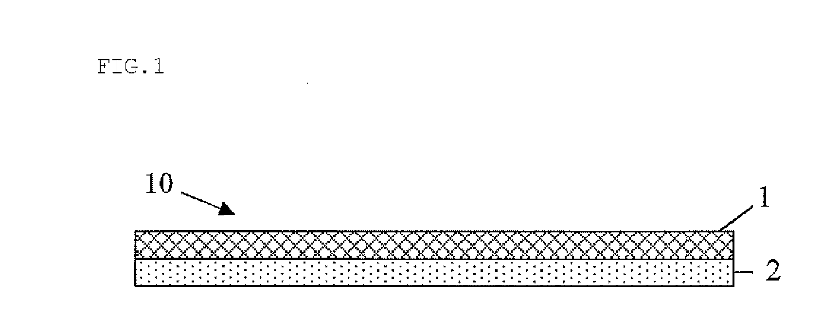
A fiber-containing resin substrate for collectively encapsulating a semiconductor-device-mounting surface of a substrate on which semiconductor devices are mounted or a semiconductor-device-forming surface of a wafer on which a semiconductor device is formed, including a resin-impregnated fibrous base material which is obtained by impregnating a fibrous base material with a thermosetting resin and semi-curing or curing the thermosetting resin and has a linear expansion coefficient (ppm/° C.) in an X-Y direction of less than 3 ppm, and an uncured resin layer formed of an uncured thermosetting resin on one side of the resin-impregnated fibrous base material.

Description

BACKGROUND OF THE INVENTION[0001]1. Field of the Invention[0002]The present invention relates to an encapsulant capable of collective encapsulation on a wafer level, particularly to an encapsulant substrate, a semiconductor-device-mounting substrate and a semiconductor-device-forming wafer that are both encapsulated with the encapsulant substrate, an individual semiconductor apparatus cut from the semiconductor-device-mounting substrate or the semiconductor-device-forming wafer, and a method for producing a semiconductor apparatus using the encapsulant substrate.[0003]2. Description of the Related Art[0004]Various methods have been proposed and studied for encapsulating, on a wafer level, a semiconductor-device-mounting surface (also simply referred to as a device-mounting surface, hereinafter) of a substrate on which semiconductor devices are mounted, or a semiconductor-device-forming surface (also simply referred to as a device-forming surface, hereinafter) of a wafer on which sem...

Claims


Application Information

Patent Timeline
IPC IPC(8): H01L23/29H01L21/56C03C25/36H01L21/78
CPCH01L23/293H01L21/78H01L21/561C03C25/36H01L23/295H01L23/3135H01L24/97H01L2224/32225H01L2224/97H01L2924/15788H01L2924/181C03C25/26C08J5/043C08J2363/04C08J2463/00B32B5/022B32B27/12B32B27/20B32B27/283B32B27/38B32B2250/02B32B2260/021B32B2260/046B32B2262/0269B32B2262/101B32B2262/103B32B2262/105B32B2262/106B32B2264/10B32B2307/306B32B2307/7265B32B2439/00B32B2457/14Y10T442/2041D06M15/41D06M15/55D06M15/643C08J5/244H01L2224/83H01L2924/00C08J7/0427C08J5/08H01L21/565
Inventor SEKIGUCHI, SUSUMUSHIOBARA, TOSHIOAKIBA, HIDEKINAKAMURA, TOMOAKI
Owner SHIN ETSU CHEM IND CO LTD
Why Eureka
Try Eureka